HCC4027B 데이터 시트보기 (PDF) - STMicroelectronics
부품명
상세내역
일치하는 목록
HCC4027B Datasheet PDF : 12 Pages
| |||
HCC/HCF4027B
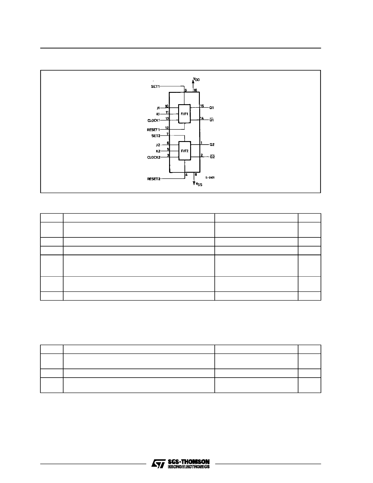
FUNCTIONAL DIAGRAM
ABSOLUTE MAXIMUM RATINGS
Symbol
Parameter
Value
Unit
V DD* Supply Voltage : HCC Types
HC F Types
– 0.5 to + 20
V
– 0.5 to + 18
V
Vi Input Voltage
II
DC Input Current (any one input)
Pt o t Total Power Dissipation (per package)
Dissipation per Output Transistor
for To p = Full Package-temperature Range
T o p Operating Temperature : HCC Types
H CF Types
– 0.5 to VDD + 0.5
V
± 10
mA
200
mW
100
mW
– 55 to + 125
°C
– 40 to + 85
°C
Ts tg Storage Temperature
– 65 to + 150
°C
Stresses above those listed under ”Absolute Maximum Ratings” may cause permanent damage to the device. This is a stress rating only
and functional operation of the device at these or any other conditions above those indicated in the operational sections of this specification
is not implied. Exposure to absolute maximum rating conditions for external periods may affect device reliability.
* All voltage values are referred to VSS pin voltage .
RECOMMENDED OPERATING CONDITIONS
Symbol
Parameter
VDD Supply Voltage : HCC Types
HC F Types
VI Input Voltage
T o p Operating Temperature : HCC Types
H CF Types
Value
3 to 18
3 to 15
0 to VDD
– 55 to + 125
– 40 to + 85
Unit
V
V
V
°C
°C
2/12
Share Link: 