CS8151(2008) 데이터 시트보기 (PDF) - ON Semiconductor
부품명
상세내역
일치하는 목록
CS8151
(Rev.:2008)
(Rev.:2008)
ON Semiconductor

CS8151 Datasheet PDF : 14 Pages
| |||
CS8151
DEFINITION OF TERMS
Dropout Voltage: The input−output voltage differential
at which the circuit ceases to regulate against further
reduction in input voltage. Measured when the output
voltage has dropped 100mV from the nominal value
obtained at 14V input, dropout voltage is dependent upon
load current and junction temperature.
Input Voltage: The DC voltage applied to the input
terminals with respect to ground.
Line Regulation: The change in output voltage for a
change in the input voltage. The measurement is made
under conditions of low dissipation or by using pulse
techniques such that the average chip temperature is not
significantly affected.
Load Regulation: The change in output voltage for a
change in load current at constant chip temperature.
Quiescent Current: The part of the positive input current
that does not contribute to the positive load current. The
regulator ground lead current.
Ripple Rejection: The ratio of the peak−to−peak input
ripple voltage to the peak−to−peak output ripple voltage.
Current Limit: Peak current that can be delivered to the
output.
CIRCUIT DESCRIPTION
Functional Description
To reduce the drain on the battery a system can go into a
low current consumption mode when ever its not performing
a main routine. The Wake Up signal is generated
continuously and is used to interrupt a microcontroller that
is in sleep mode. The nominal output is a 5.0 V square wave
with a duty cycle of 50% at a frequency that is determined
by a timing capacitor, CDelay.
When the microprocessor receives a rising edge from the
Wake Up output, it must issue a watchdog pulse and check
its inputs to decide if it should resume normal operations or
remain in the sleep mode.
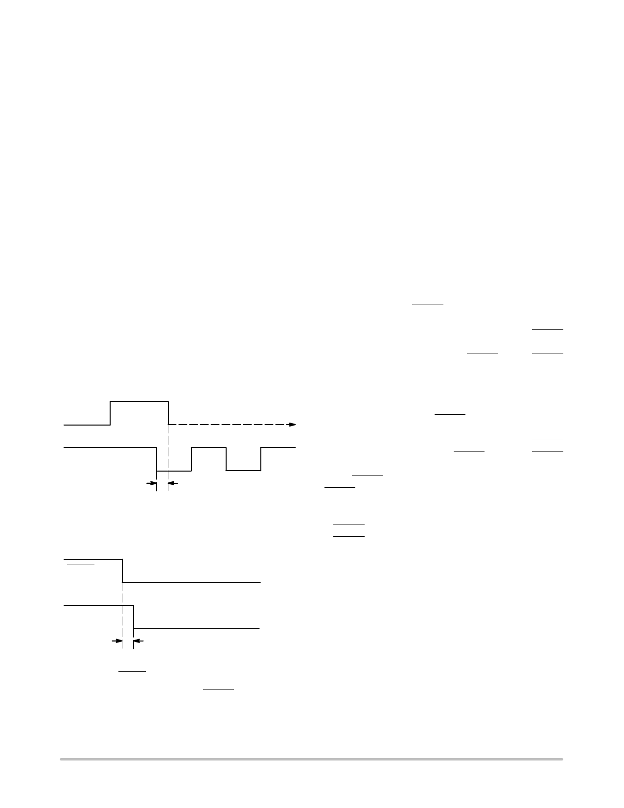
Wake Up
WDI
Wake Up
Response
to WDI
Figure 5. Wake Up Response to WDI
RESET
The first falling edge of the watchdog signal causes the
Wake Up to go low within 2.0 ms (Typ) and remain low until
the next Wake Up cycle (see Figure 5). Other watchdog
pulses received within the same cycle are ignored (Figures
2, 3, and 4).
During power up, RESET is held low until the output
voltage is in regulation. During operation, if the output
voltage shifts below the regulation limits, the RESET
toggles low and remains low until proper output voltage
regulation is restored. After the RESET delay, RESET
returns high.
The Watchdog circuitry continuously monitors the input
watchdog signal (WDI) from the microprocessor. The
absence of a falling edge on the Watchdog input during one
Wake Up cycle will cause a RESET pulse to occur at the end
of the Wake Up cycle (see Figure 3).
The Wake Up output is pulled low during a RESET
regardless of the cause of the RESET. After the RESET
returns high, the Wake Up cycle begins again (see Figure 3).
The RESET pulse width, Wake Up signal frequency and
RESET high to Wake Up delay time are all set by one
external capacitor CDelay.
Wake Up Period = (4 × 10⁵)CDelay
RESET Delay Time = (5 × 10⁴)CDelay
RESET High to Wake Up Delay Time = (2 × 10⁵)CDelay
Capacitor temperature coefficient and tolerance as well as
the tolerance of the CS8151 must be taken into account in
order to get the correct system tolerance for each parameter.
Wake Up
Wake Up
Response
to RESET
Figure 6. Wake Up Response to RESET (Low Voltage)
http://onsemi.com
7
Share Link: