SL74HC109 데이터 시트보기 (PDF) - System Logic Semiconductor
부품명
상세내역
일치하는 목록
SL74HC109
System Logic Semiconductor

SL74HC109 Datasheet PDF : 5 Pages
| |||
SL74HC109
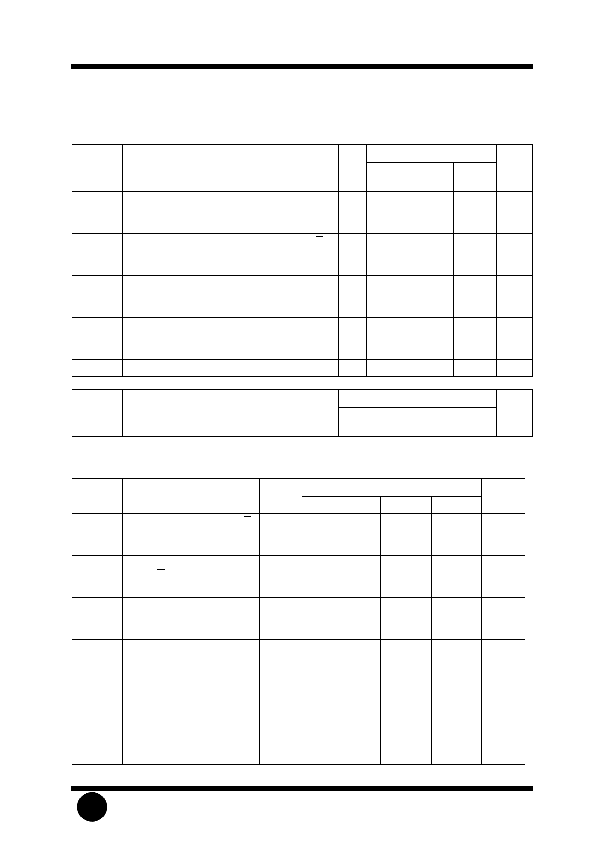
A C E L E C T R I C A L C H A R A C T E R I S T I C S (CL=50pF,Input tr=tf=6.0 ns)
VCC
Guaranteed Limit
Symbol
Parameter
V 25 °C to ≤85°C ≤125°C Unit
-55°C
fm a x
Maximum Clock Frequency (50% Duty Cycle)
(Figures 1 and 4)
2.0
6
4.8
4.0 MHz
4.5 30
24
20
6.0 35
28
24
tPLH, tPHL Maximum Propagation Delay, Clock to Q or Q
(Figures 1 and 4)
2.0 175
220
265
ns
4.5 35
44
53
6.0 30
37
45
tPLH, tPHL Maximum Propagation Delay , Set or Reset to Q or 2.0 230
290
345
ns
Q (Figures 2 and 4)
4.5 46
58
69
6.0 39
49
59
tTLH, tTHL Maximum Output Transition Time, Any Output
2.0 75
95
110
ns
(Figures 1 and 4)
4.5 15
19
22
6.0 13
16
19
CI N
Maximum Input Capacitance
-
10
10
10
pF
Power Dissipation Capacitance (Per Flip-Flop)
CPD Used to determine the no-load dynamic power
consumption: PD=CPDVCC2f+ICCVCC
Typical @25°C,VCC=5.0 V
40
pF
T I M I N G R E Q U I R E M E N T S (CL=50pF,Input tr=tf=6.0 ns)
VCC
Symbol
Parameter
V
tSU
Minimum Setup Time, J or K to 2.0
Clock (Figure 3)
4.5
6.0
th
Minimum Hold Time, Clock to
2.0
J or K (Figure 3)
4.5
6.0
trec
Minimum Recovery Time, Set
2.0
or Reset Inactive to Clock
4.5
(Figure 2)
6.0
tw
Minimum Pulse Width, Set or
2.0
Reset (Figure 2)
4.5
6.0
tw
Minimum Pulse Width,Clock
2.0
(Figure 1)
4.5
6.0
tr, tf
Maximum Input Rise and Fall
2.0
Times (Figure 1)
4.5
6.0
Guaranteed Limit
25 °C to -55°C ≤85°C ≤125°C Unit
100
125
150
ns
20
25
30
17
21
26
5
5
5
ns
5
5
5
5
5
5
5
5
5
ns
5
5
5
5
5
5
80
100
12
ns
16
20
24
14
17
20
80
100
12
ns
16
20
24
14
17
20
1000
1000
1000
ns
500
500
500
400
400
400
S L S System Logic
Semiconductor
Share Link: