MC33143DW 데이터 시트보기 (PDF) - Motorola => Freescale
부품명
상세내역
일치하는 목록
MC33143DW Datasheet PDF : 8 Pages
| |||
Freescale SMeCm33i1c4o3nductor, Inc.
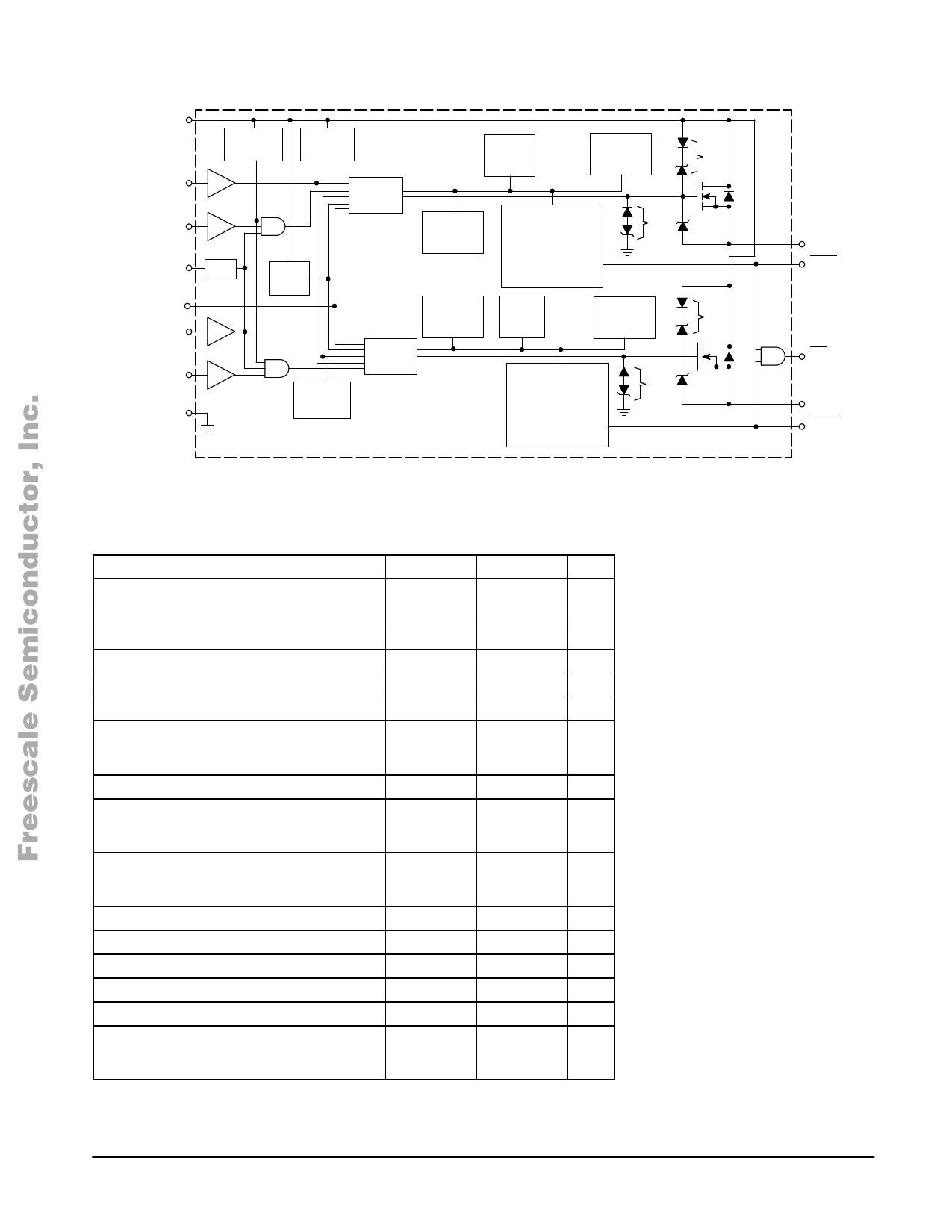
VPwr (9, 16)
SFPD (14)
IN1 (1)
VDD (11)
GTST (15)
CEN (2)
IN2 (12)
Gnd (5) (See Note)
Figure 1. Simplified Internal Block Diagram
Overvoltage
Shutdown
Voltage
Regulator
Gate
Control
Bias
Charge
Pump
4.0 ms
Retry Timer
Gate
Control
Current
Limit
Over
Temperature
Shutdown
55 V
OFF/ON
Open Load
Detect
OFF/ON
Open Load
Detect
Fault Detection
D ON/OFF Open Load
D
D
ON/OFF VPwr Short
On Ground Short
D Over Temperature
D VPwr Overvoltage
–10 V 15 V
Current
Limit
Over
Temperature
55 V
Shutdown
Fault Detection
D ON/OFF Open Load
D
D
ON/OFF VPwr Short
On Ground Short
D Over Temperature
D VPwr Overvoltage
–10 V 15 V
OUT1 (24)
STAT1 (3)
INT (23)
OUT2 (13)
STAT2 (10)
NOTE: Pins 5, 6, 7, 8, 17, 18, 19 and 20 should all be grounded so as to provide electrical as well as thermal heatsinking of the device.
MAXIMUM RATINGS (All voltages are with respect to ground, unless otherwise noted.)
Rating
Power Supply Voltage
ÁÁÁÁÁÁÁÁÁÁÁÁÁÁÁÁÁÁÁÁÁÁÁÁÁÁÁÁÁÁÁÁÁÁÁÁÁÁÁÁÁÁÁÁÁÁ Steady State Continuous Operation
Symbol
VPwr
Value
Unit
V
26
Negative Transient (Note 1)
–1.5
Positive Load Dump Transient (Note 2)
Logic Supply Voltage Range
ÁÁÁÁÁÁÁÁÁÁÁÁÁÁÁÁÁÁÁÁÁÁÁ Logic Supply Current
ÁÁÁÁÁÁÁÁÁÁÁÁÁÁÁÁÁÁÁÁÁÁÁ Input Voltage (Note 3)
ÁÁÁÁÁÁÁÁÁÁÁÁÁÁÁÁÁÁÁÁÁÁÁ Output Clamp Voltage
ÁÁÁÁÁÁÁÁÁÁÁÁÁÁÁÁÁÁÁÁÁÁÁ IO = –20 mA
ÁÁÁÁÁÁÁÁÁÁÁÁÁÁÁÁÁÁÁÁÁÁÁ IO = –200 mA
ÁÁÁÁÁÁÁÁÁÁÁÁÁÁÁÁÁÁÁÁÁÁÁ Output Current Limit (Note 4)
ÁÁÁÁÁÁÁÁÁÁÁÁÁÁÁÁÁÁÁÁÁÁÁ Output Clamp Energy (IO = –1.0 A)
TJ = 25°C
ÁÁÁÁÁÁÁÁÁÁÁÁÁÁÁÁÁÁÁÁÁÁÁ TJ = 125°C
VDD
IDD
Vin
VClamp
IO(Lim)
EClamp
60
–0.3 to 7.0
V
5.0
mA
–0.3 to 7.0
V
V
–3.0 to –20
–5.5 to –20
–3.0 to –6.0
A
mJ
300
100
NOTES: 1. Negative transient survival capability
for 100 ms time duration.
2. Positive transient survival capability
with typical automotive load dump
condition; 400 ms time constant
decay.
ESD (Minimum)
V
Human Body Model (Note 5)
Machine Model (Note 6)
ÁÁÁÁÁÁÁÁÁÁÁÁÁÁÁÁÁÁÁÁÁÁÁ Power Dissipation (TA = 25°C) (Note 7)
ÁÁÁÁÁÁÁÁÁÁÁÁÁÁÁÁÁÁÁÁÁÁÁ Operating Temperature (Note 8)
ÁÁÁÁÁÁÁÁÁÁÁÁÁÁÁÁÁÁÁÁÁÁÁ Operating Junction Temperature
ÁÁÁÁÁÁÁÁÁÁÁÁÁÁÁÁÁÁÁÁÁÁÁ Storage Temperature
ÁÁÁÁÁÁÁÁÁÁÁÁÁÁÁÁÁÁÁÁÁÁÁ Soldering Temperature (for 10 Seconds)
ÁÁÁÁÁÁÁÁÁÁÁÁÁÁÁÁÁÁÁÁÁÁÁÁÁÁÁÁÁÁÁÁÁÁÁÁÁÁÁÁÁÁÁÁÁÁ Thermal Resistance
HBM
MM
PD
TA
TJ
Tstg
Tsolder
2000
200
4.2
–40 to +125
–40 to +150
–55 to +150
270
W
°C
°C
°C
°C
°C/W
Junction–to–Lead
RθJL
15
3. All input pins (IN1–2, CEN and
SFPD).
4. Each output has independent
current limiting.
5. Performed in accordance to HBM;
CZap = 100 pF, RZap = 1500 Ω.
6. Performed in accordance to MM;
CZap = 100 pF, RZap = 0 Ω.
7. Derate Power Dissipation 33 mW/°C
for temperatures above 25°C.
8. Ambient temperature is given as a
practical reference; Maximum
junction temperature is the limiting
factor.
Junction–to–Ambient
RθJA
30
9. ESD data available upon request.
2
MOTOROLA ANALOG IC DEVICE DATA
For More Information On This Product,
Go to: www.freescale.com
Share Link: 