NCP1216AD100R2G(2010) 데이터 시트보기 (PDF) - ON Semiconductor
부품명
상세내역
일치하는 목록
NCP1216AD100R2G
(Rev.:2010)
(Rev.:2010)
ON Semiconductor

NCP1216AD100R2G Datasheet PDF : 18 Pages
| |||
NCP1216, NCP1216A
3. Implement Figure 3, from AN8069/D, Solution: This is
another possible option to keep the DSS functionality (good
short−circuit protection and EMI jittering) while driving any
types of MOSFETs. This solution is recommended when the
designer plans to use SOIC−8 controllers.
4. Connect an Auxiliary Winding: If the mains conditions
are such that you simply can’t match the maximum power
dissipation, then you need to connect an auxiliary winding
to permanently disconnect the startup source.
Overload Operation
In applications where the output current is purposely not
controlled (e.g. wall adapters delivering raw DC level), it is
interesting to implement a true short−circuit protection. A
short−circuit actually forces the output voltage to be at a low
level, preventing a bias current to circulate in the
Optocoupler LED. As a result, the FB pin level is pulled up
to 4.2 V, as internally imposed by the IC. The peak current
setpoint goes to the maximum and the supply delivers a
rather high power with all the associated effects. Please note
that this can also happen in case of feedback loss, e.g. a
broken Optocoupler. To account for this situation, NCP1216
hosts a dedicated overload detection circuitry. Once
activated, this circuitry imposes to deliver pulses in a burst
manner with a low duty−cycle. The system auto−recovers
when the fault condition disappears.
During the startup phase, the peak current is pushed to the
maximum until the output voltage reaches its target and the
feedback loop takes over. This period of time depends on
normal output load conditions and the maximum peak
current allowed by the system. The time−out used by this IC
works with the VCC decoupling capacitor: as soon as the
VCC decreases from the VCCOFF level (typically 12.2 V) the
device internally watches for an overload current situation.
If this condition is still present when the VCCON level is
reached, the controller stops the driving pulses, prevents the
self−supply current source to restart and puts all the circuitry
in standby, consuming as little as 350 mA typical (ICC3
parameter). As a result, the VCC level slowly discharges
toward 0 V. When this level crosses 5.6 V typical, the
controller enters a new startup phase by turning the current
source on: VCC rises toward 12.2 V and again delivers
output pulses at the VCCOFF crossing point. If the fault
condition has been removed before VCCON approaches,
then the IC continues its normal operation. Otherwise, a new
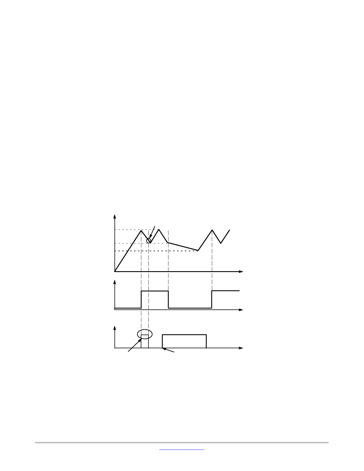
fault cycle takes place. Figure 25 shows the evolution of the
signals in presence of a fault.
VCC
12.2 V
10 V
5.6 V
Regulation
Occurs Here
Latchoff
Phase
Time
Drv
VCCOFF = 12.2 V
VCCON = 10 V
VCClatch = 5.6 V
Internal
Fault Flag
Driver
Pulses
Driver
Pulses
Time
Startup Phase
Fault is
Relaxed
Fault Occurs Here
Time
Figure 25.
If the fault is relaxed during the VCC natural fall down
sequence, the IC automatically resumes.
If the fault still persists when VCC reached VCCON, then the
controller cuts everything off until recovery.
Calculating the VCC Capacitor
As the above section describes, the fall down sequence
depends upon the VCC level: how long does it take for the
VCC line to go from 12.2 V to 10 V. The required time
http://onsemi.com
13
Share Link: