NCP1217P65G(2010) 데이터 시트보기 (PDF) - ON Semiconductor
부품명
상세내역
일치하는 목록
NCP1217P65G
(Rev.:2010)
(Rev.:2010)
ON Semiconductor

NCP1217P65G Datasheet PDF : 19 Pages
| |||
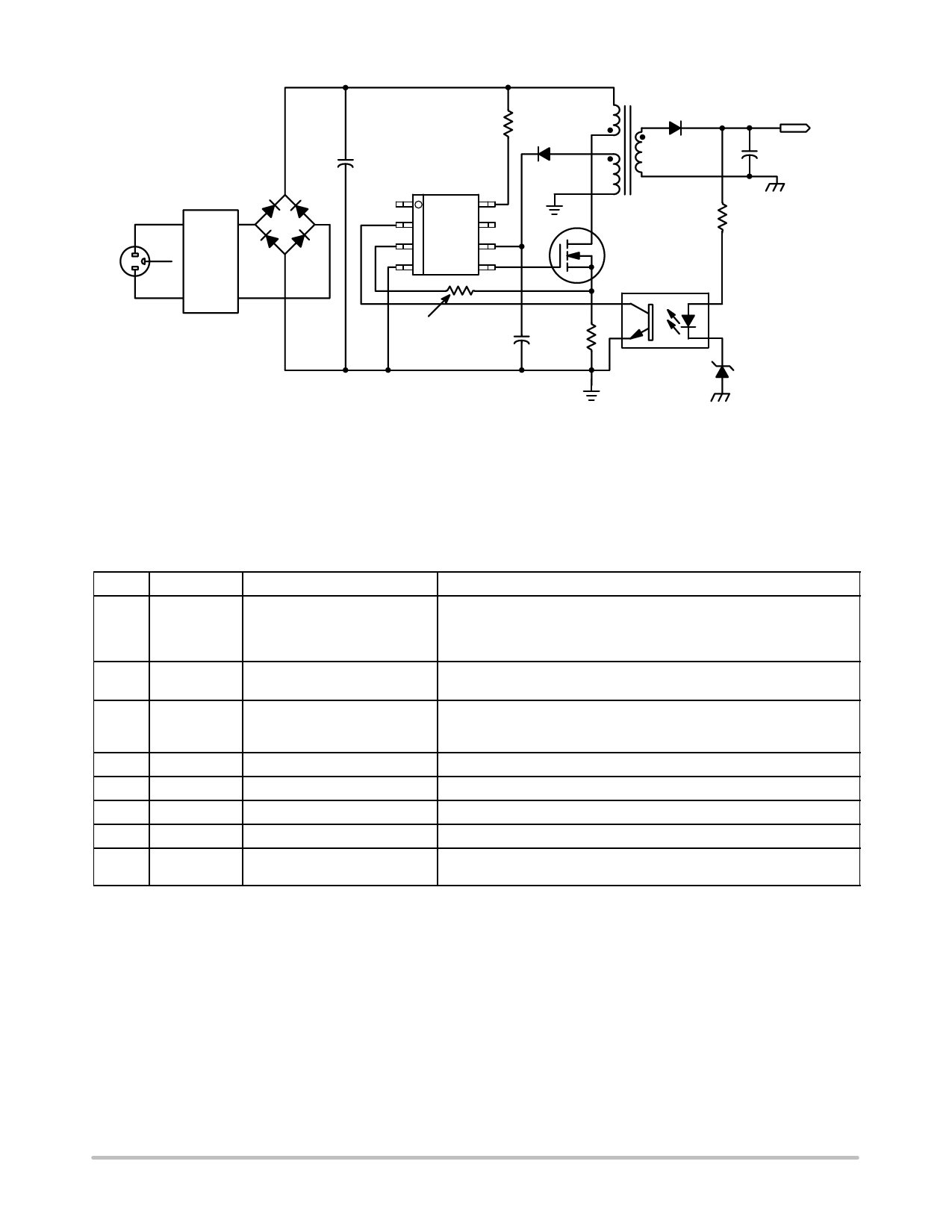
EMI
FILTER
UNIVERSAL
INPUT
NCP1217, NCP1217A
See Application
Section
+
NCP1217
1 Adj HV 8
2 FB
7
3 CS VCC 6
Gnd Drv
4
5
Aux.
Ramp Adjustment +
Figure 1. Typical Application Example
VOUT
+
PIN FUNCTION DESCRIPTION
Pin No. Pin Name
Function
1
Adj
Adjust the skipping peak current
2
FB
Sets the peak current setpoint
3
CS
Current sense input
4
GND
The IC ground
5
Drv
Driving pulses
6
VCC
Supplies the IC
7
NC
--
8
HV
Ensures a clean and lossless
startup sequence
Description
This pin lets you adjust the level at which the cycle skipping process takes
place. Shorting this pin to ground permanently disables the skip cycle
feature.
By bringing this pin above 3.1 V, you permanently shut off the device.
By connecting an optocoupler to this pin, the peak current setpoint is ad-
justed accordingly to the output power demand.
This pin senses the primary current and routes it to the internal comparat-
or via an L.E.B. By inserting a resistor in series with the pin, you control
the amount of ramp compensation you need.
--
The driver’s output to an external MOSFET.
This pin is connected to an external bulk capacitor of typically 22 mF.
This unconnected pin ensures adequate creepage distance.
Connected to the high--voltage rail, this pin injects a constant current into
the VCC capacitor during the startup sequence.
http://onsemi.com
2
Share Link: