74HC377N(2013) 데이터 시트보기 (PDF) - NXP Semiconductors.
부품명
상세내역
일치하는 목록
74HC377N
(Rev.:2013)
(Rev.:2013)
NXP Semiconductors.

74HC377N Datasheet PDF : 20 Pages
| |||
NXP Semiconductors
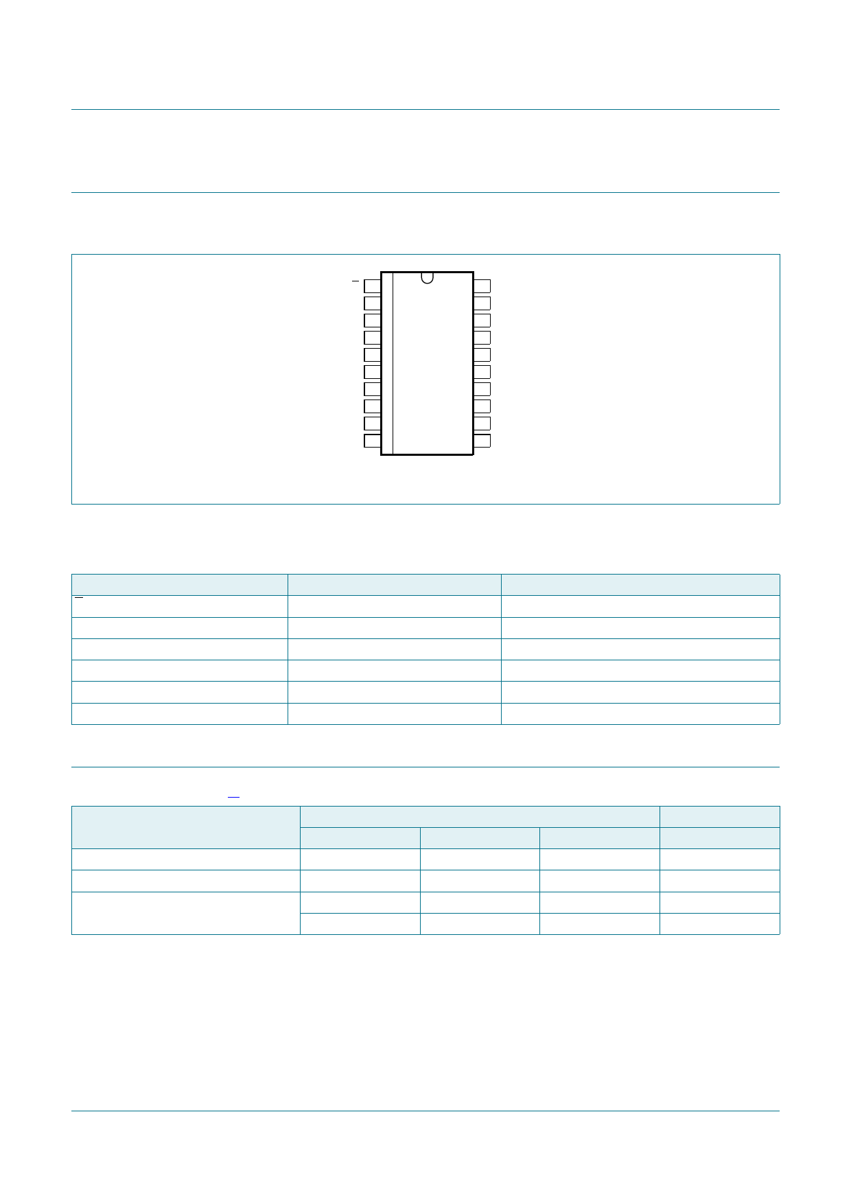
5. Pinning information
5.1 Pinning
74HC377; 74HCT377
Octal D-type flip-flop with data enable; positive-edge trigger
Fig 5. Pin configuration
E1
Q0 2
D0 3
D1 4
Q1 5
Q2 6
D2 7
D3 8
Q3 9
GND 10
20 VCC
19 Q7
18 D7
17 D6
16 Q6
377
15 Q5
14 D5
13 D4
12 Q4
11 CP
mna917
5.2 Pin description
Table 2. Pin description
Symbol
E
Q0, Q1, Q2, Q3, Q4, Q5, Q6, Q7
D0, D1, D2, D3, D4, D5, D6, D7
GND
CP
VCC
Pin
1
2, 5, 6, 9, 12, 15, 16, 19
3, 4, 7, 8, 13, 14, 17, 18
10
11
20
6. Functional description
Description
data enable input (active LOW)
flip-flop output
data input
ground (0 V)
clock input (LOW-to-HIGH, edge triggered)
supply voltage
Table 3. Function table[1]
Operating modes
Inputs
CP
E
Dn
load “1”
l
h
load “0”
l
l
hold (do nothing)
h
X
X
H
X
[1] H = HIGH voltage level;
h = HIGH voltage level one set-up time prior to the LOW-to-HIGH clock transition;
L = LOW voltage level;
l = LOW voltage level one set-up time prior to the LOW-to-HIGH clock transition;
X = don’t care;
= LOW-to-HIGH clock transition.
Outputs
Qn
H
L
no change
no change
74HC_HCT377
Product data sheet
All information provided in this document is subject to legal disclaimers.
Rev. 3 — 25 September 2013
© NXP B.V. 2013. All rights reserved.
4 of 19
Share Link: