SL4013B 데이터 시트보기 (PDF) - System Logic Semiconductor
부품명
상세내역
일치하는 목록
SL4013B Datasheet PDF : 5 Pages
| |||
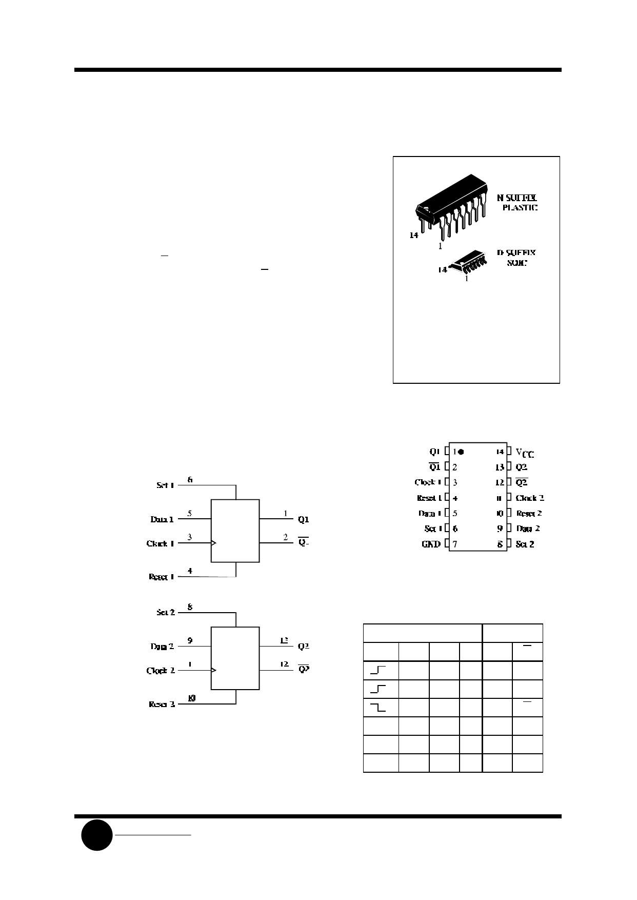
SL4013B
Dual D Flip-Flop
High-Voltage Silicon-Gate CMOS
The SL4013B consists of two identical, independent data-type flip-
flops. Each flip-flop has independent data, set, reset, and clock inputs
and Q and Q outputs. These devices can be used for shift register
applications, and, by connecting Q output to the data input, for
counter and toggle applications. The logic level present at the D input
is transferred to the Q output during the positive-going transition of
the clock pulse. Setting or resetting is independent of the clock and is
accomplished by a high level on the set or reset line, respectively.
• Operating Voltage Range: 3.0 to 18 V
• Maximum input current of 1 µA at 18 V over full package-
temperature range; 100 nA at 18 V and 25°C
• Noise margin (over full package temperature range):
1.0 V min @ 5.0 V supply
2.0 V min @ 10.0 V supply
LOGIC DIAGRAM
ORDERING INFORMATION
SL4013BN Plastic
SL4013BD SOIC
TA = -55° to 125° C for all packages
PIN ASSIGNMENT
PIN 14 =VCC
PIN 7 = GND
SLS
System Logic
Semiconductor
2.5 V min @ 15.0 V supply
FUNCTION TABLE
Inputs
Clock Data Reset Set
L LL
H LL
X LL
X X HL
X X LH
X X HH
Outputs
QQ
LH
HL
QQ
LH
HL
HH
X = don’t care
Share Link: 