L4902A 데이터 시트보기 (PDF) - STMicroelectronics
부품명
상세내역
일치하는 목록
L4902A Datasheet PDF : 9 Pages
| |||
L4902A
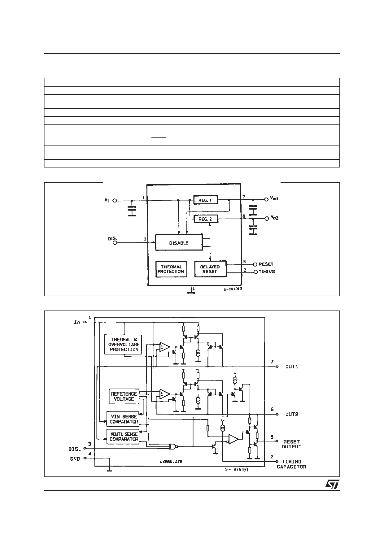
PIN FUNCTIONS
N°
Name
Function
1
Input 1
Regulators Common Input
2
Timing
If Reg. 2 is switched-ON the delay capacitor is charged with a 5µA constant current. When
Capacitor Reg. 2 is switched-OFF the delay capacitor is discharged.
3 Disable Input A high level (> VDT) disable output Reg. 2.
4
GND
Common Ground
5 Reset Output When pin 2 reaches 5V the reset output is switched high.
Therefore
tRD
=
Ct
( 5V )
10µA
;
tRD
(ms)
=
Ct
(nF)
6
Output 2 5V – 300mA Regulator Output. Enabled if Vo 1 > VRT. DISABLE INPUT < VDT and VIN > VIT. If
Reg. 2 is switched-OFF the C02 capacitor is discharged.
7
Output 1 5V – 300mA. Low leakage (in switch-OFF condition) output
BLOCK DIAGRAM
SCHEMATIC DIAGRAM
2/9
Share Link: 