SL74HC75D 데이터 시트보기 (PDF) - System Logic Semiconductor
부품명
상세내역
일치하는 목록
SL74HC75D Datasheet PDF : 5 Pages
| |||
SL74HC75
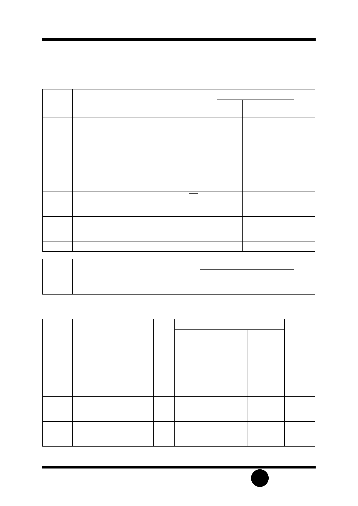
AC ELECTRICAL CHARACTERISTICS(CL=50pF,Input tr=tf=6.0 ns)
Symbol
Parameter
tPLH, tPHL Maximum Propagation Delay, D to Q (Figures 1
and 5)
tPLH, tPHL Maximum Propagation Delay , D to Q
(Figures 1 and 5)
tPLH, tPHL Maximum Propagation Delay ,Latch Enable to Q
(Figures 2 and 5)
tPLH, tPHL Maximum Propagation Delay ,Latch Enable to Q
(Figures 2 and 5)
tTLH, tTHL Maximum Output Transition Time, Any Output
(Figures 3 and 5)
CIN
Maximum Input Capacitance
VCC
Guaranteed Limit
V 25 °C to ≤85°C ≤125°C Unit
-55°C
2.0 125
155
190
ns
4.5 25
31
38
6.0 21
26
32
2.0 110
140
165
ns
4.5 22
28
33
6.0 19
24
28
2.0 145
180
220
ns
4.5 29
36
44
6.0 25
31
38
2.0 125
155
190
ns
4.5 25
31
38
6.0 21
26
32
2.0 75
95
110
ns
4.5 15
19
22
6.0 13
16
19
-
10
10
10
pF
Power Dissipation Capacitance (Per Latch)
CPD Used to determine the no-load dynamic power
consumption:
PD=CPDVCC2f+ICCVCC
Typical @25°C,VCC=5.0 V
35
pF
TIMING REQUIREMENTS (CL=50pF,Input tr=tf=6.0 ns)
Symbol
Parameter
VCC
Guaranteed Limit
V
25 °C to
≤85°C
≤125°C
Unit
-55°C
tSU
Minimum Setup Time,
2.0
100
125
150
ns
Input D to Latch Enable
4.5
20
25
30
(Figure 4)
6.0
17
21
26
th
Minimum Hold Time,Latch
2.0
25
30
40
ns
Enable to D (Figure 4)
4.5
5
6
8
6.0
5
6
7
tw
Minimum Pulse Width, Latch
2.0
80
Enable Input
4.5
16
(Figure 2)
6.0
14
100
120
ns
20
24
17
20
tr, tf Maximum Input Rise and Fall
2.0
1000
1000
1000
ns
Times (Figure 1)
4.5
500
500
500
6.0
400
400
400
SLS
System Logic
Semiconductor
Share Link: 