ZSD100N8 데이터 시트보기 (PDF) - Diodes Incorporated.
부품명
상세내역
일치하는 목록
ZSD100N8 Datasheet PDF : 8 Pages
| |||
ZSD100
Improved Frequency Control
ZSD100
RT
VCC
_
SAW
Q
RT
C MOD
Q
G ND
C OUT
VCC
CMOD
COUT
GND
Improved frequency control can be achieved with an external resistor between the RT pin and GND.
An external resistor reduces the value of the timing capacitors required for the selected operating
frequency and also reduces the ZSD100’s power consumption.
Note: The outputs of the ZSD100 have been designed to avoid cross-conduction in full bridge output
circuits. Large value external timing resistors can lead to a small level of cross-conduction. It is
recommended that external timing resistors are not used with bridge output circuits.
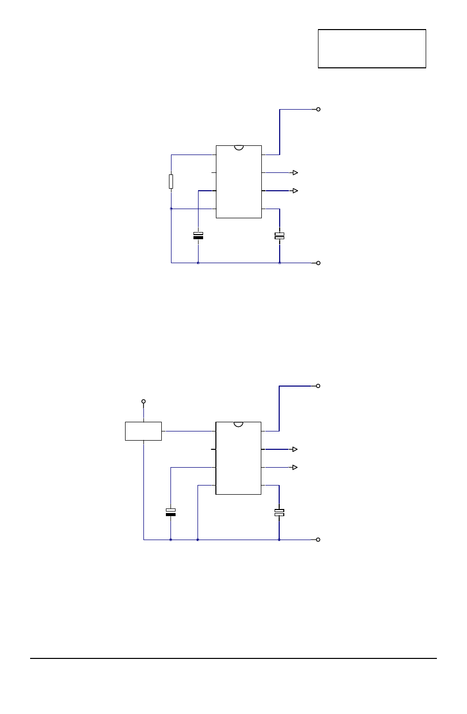
Remote Switching
If the RT pin is switched open-circuit, all internal functions of the IC are shut down.
Logic supply
VCC
LOGIC
Open
collector
output
ZSD100
RT
VCC
_
SAW
Q
CMOD
Q
GND
C OUT
CMOD
COUT
GND
Note: A small leakage current in the open collector logic controller will enable the IC. If such leakage
cannot be eliminated, its effect can be easily negated by adding a high value resistor (eg. 100k)
between pin RT and VCC. This resistor will have no effect on frequency control.
Issue 8 - June 2007
© Zetex Semiconductors plc 2007
www.zetex.com
Share Link: 