PCK2011DL 데이터 시트보기 (PDF) - Philips Electronics
부품명
상세내역
일치하는 목록
PCK2011DL Datasheet PDF : 11 Pages
| |||
Philips Semiconductors
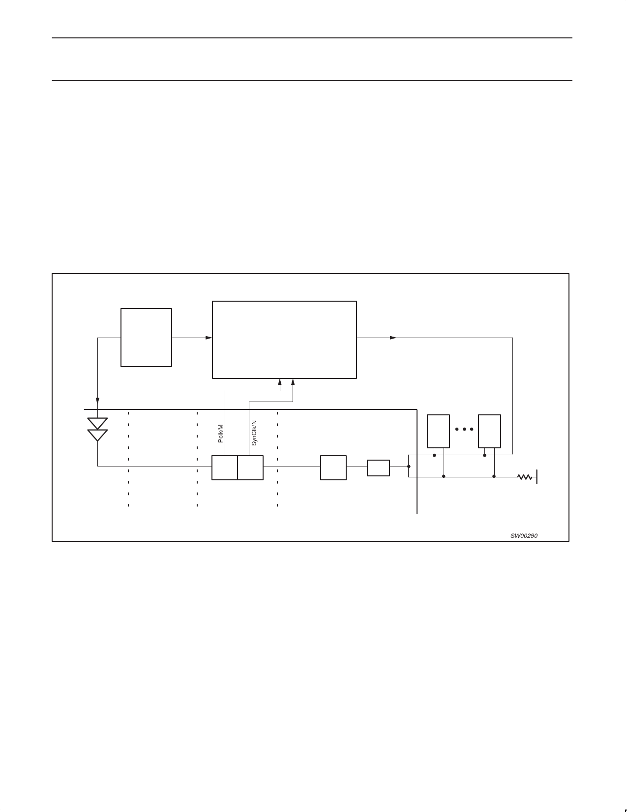
Direct Rambus™ Clock Generator
Preliminary specification
PCK2011
This configuration achieves frequency-lock between the controller
and Rambus Channel clocks (PCLK and SYNCLK). These clock
signals are matched and phase-aligned at the RMC/RAC boundary
in order to allow data transfers to occur across this boundary without
additional latency.
The main clock source drives the system clock (PCLK) to the ASIC,
and also drives the reference clock (REFCLK) to the DRCG.
REFCLK may or may not be the same frequency as PCLK. A PLL
inside the DRCG multiplies REFCLK to generate the desired
frequency for BUSCLK. BUSCLK is driven on the Rambus Channel
through a terminated transmission line. At the mid-point of the
Channel, the RAC senses BUSCLK using its own DLL for clock
alignment, followed by a fixed divide-by- 4 circuit that generates
SYNCLK.
Pclk is the clock used in the Rambus memory controller (RMC) in
the ASIC. SYNCLK is the clock used at the ASIC interface of the
RAC. The DRCG together with the Gear Ratio Logic enables the
controller to exchange data directly from the PCLK domain to the
SYNCLK domain without incurring additional latency for
synchronization. In general, PCLK and SYNCLK can run at different
frequencies, so the Gear Ratio Logic must select the appropriate M
and N dividers such that the frequencies of PCLK/M and SYNCLK/N
are equal. In one example, PCLK=133MHz and SYNCLK=100MHz,
and M=4 while N=3, giving PCLK/M = SYNCLK/N = 33MHz. Figure
4 shows an example of the clock waveforms generated with the
Gear Ratio Logic.
PCK2010
REFCLK
Direct Rambus
Clock Generator
(DRCG)
BUSCLK
RMC
RAC
RDRAMs
PCLK
M
N
Gear Ratio-
Logic
CONTROLLER
/4
DLL
SYNCLK
Figure 1. System Clock Architecture
SW00290
The ASIC drives the output clocks, Pclk and SynClk/N from the
Gear Ratio Logic to the DRCG Phase Detector inputs. The routing
of the Pclk/M and SynClk/N signal traces must be matched in
impedance and propagation delay on the ASIC as well as on the
board. These signals are not part of the Rambus Channel and their
routing must be matched by board designers.
After comparing the phases of Pclk/M and SynClk/N, the DRCG
Phase Detector drives a phase aligner that adjusts the phase of
DRCG output clock, Busclk. Since the other elements in the
distributed loop have a fixed delay, adjusting Busclk adjusts the
phase of SynClk and thus the phase of SynClk/N.
In this manner, the distributed loop adjusts the phase of SynClk/N to
match that of Pclk/M, eliminating the phase error at the input of the
DRCG. When the clocks are aligned, data can be exchanged
directly from the Pclk domain to the SynClk domain.
The Gear Ratio Logic supports four clock ratios (2.0, 1.5, 1.33, and
1.0), where the ratio is defined as the ratio of Pclk/SynClk. Since
Busclk = 4*SynClk, this ratio also is equal to 4*Pclk/Busclk. Other
ratios could be used, depending on particular system
implementations.
1999 Jan 19
4
Share Link: 