NJU8402 데이터 시트보기 (PDF) - Japan Radio Corporation
부품명
상세내역
일치하는 목록
NJU8402 Datasheet PDF : 10 Pages
| |||
NJU8402
s FUNCTION DESCRIPTION
(1-1) Analog Audio Signal Output
Analog signal output is biased in the chip and the maximum amplitude is 0.56 × AVDD. The internal
switched capacitor Low Pass Filter is so effective that the external Low Pass Filters are required only 2-
pole LPF or 3-pole.
(1-2) Serial Data Interface
DIN (Data Input), BCLK (Bit Clock) and LRCK (L/R Clock) are the serial data interface terminals. BCLK is
the bit clock of audio data and IO data are leaded at raising edge of the BCLK. The signal into LRCK
terminal represents the signal for distinguishing between Lch and Rch, and the signal for starting data. The
frequency of LRCK is sampling rate of system ( fs ). The MCIK must be synchronized with LRCK and is
256 times or 384 of fs. The serial data format is complement of 2, MSB-first and compatible with I2S serial
data protocol or LSB justified. This serial data format is set by the control register.
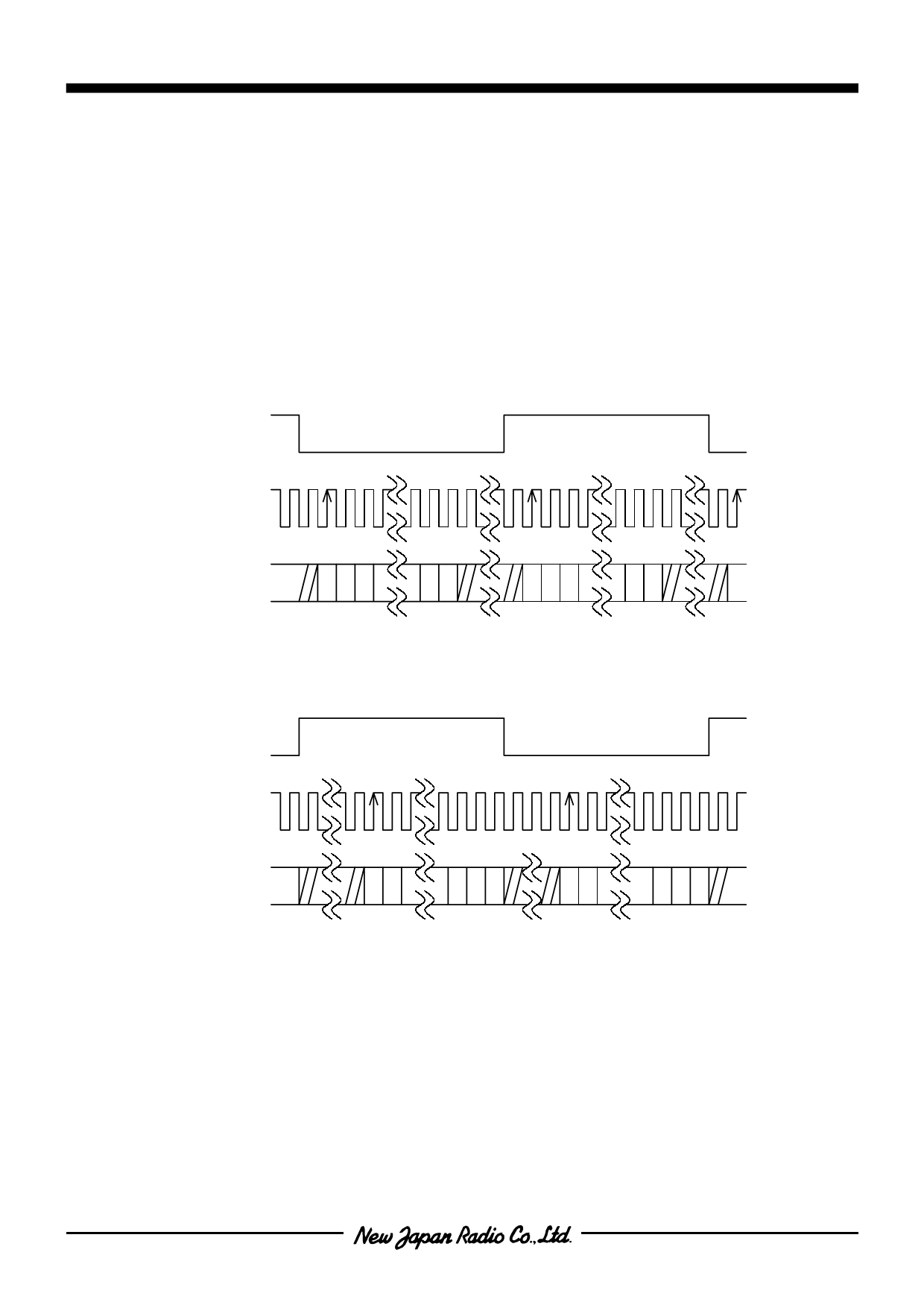
LRCK
Left
Right Channel
BCLK
DIN
15 14 13
10
15 14 13
10
I2S serial data format
LRCK
Left
Right Channel
BCLK
DIN
0
15 14
210
15 14
LSB justified serial data format
210
(1-3) System Clock
System Clock into the MCIK terminal must be 256 times or 384 times of fs and synchronizing with LRCK.
This frequency is set by the control register.
(1-4) Reset
The external reset is the asynchronous reset. Reset is released at the falling edge at LRCK. Reset by
command is synchronous which operates as same as the external reset function.
-3-
Share Link: 