XC9110A451ER 데이터 시트보기 (PDF) - TOREX SEMICONDUCTOR
부품명
상세내역
일치하는 목록
XC9110A451ER Datasheet PDF : 35 Pages
| |||
XC9110/XC9111 Series
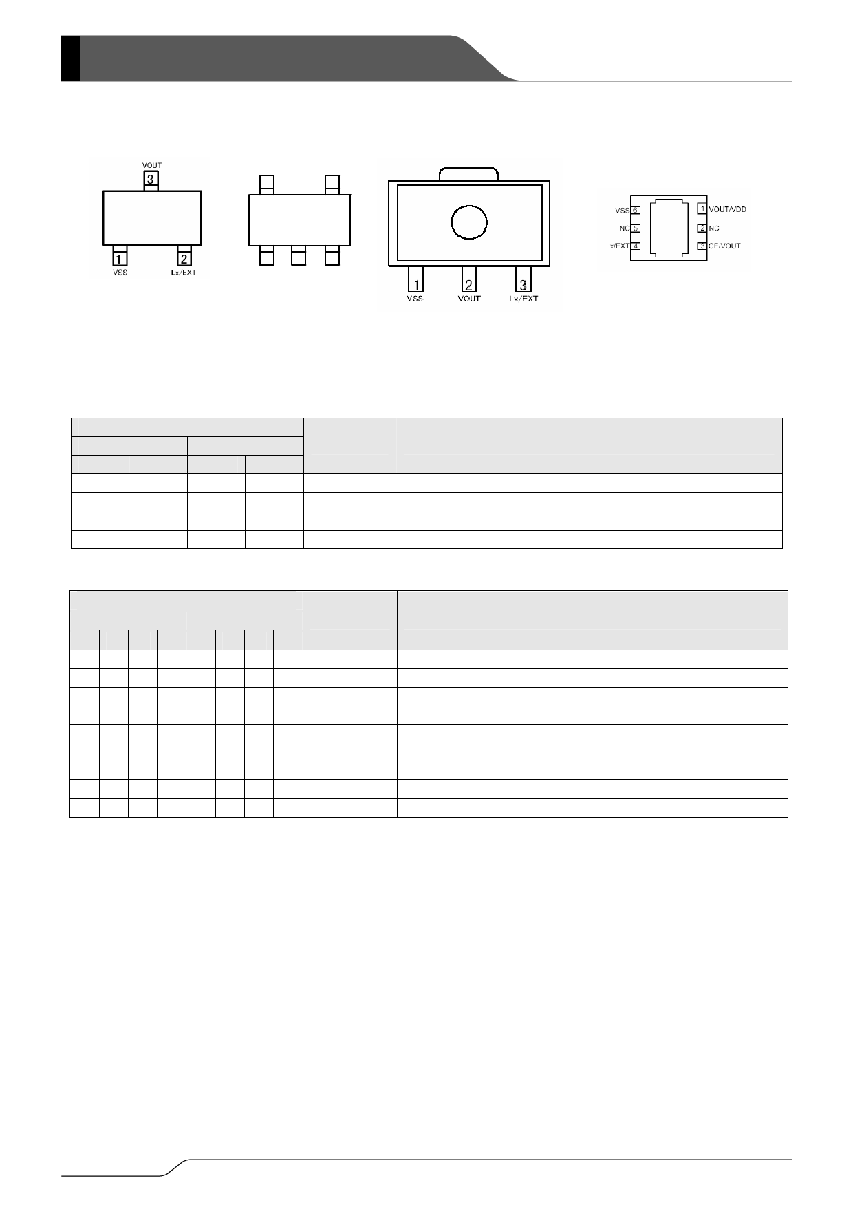
■PIN CONFIGURATION
Lx /EXT
V SS
5
4
SOT-23 (TOP VIEW)
1
2
3
CE/V OUT V OUT/V DD NC
SOT-25 (TOP VIEW)
■PIN ASSIGNMENT
●XC9111A/B
PIN NUMBER
SOT-23
SOT-89
A
B
A
B
1
1
1
1
3
3
2
2
2
-
3
-
-
2
-
3
PIN NAME
VSS
VOUT
LX
EXT
SOT-89 (TOP VIEW)
USP-6C (BOTTOM VIEW)
*The dissipation pad for the USP-6C package
should be solder-plated in recommended mount
pattern and metal masking so as to enhance
mounting strength and heat release. If the pad
needs to be connected to other pins, it should be
connected to the pin No.1.
FUNCTIONS
: Ground
: Output Voltage Montior, Internal Power Supply
: Switch
: External Switching transistor drive <N-ch transistor drive)
●XC9110//9111C/D/E/F
PIN NUMBER
SOT-25
USP-6C
CDE F CDE F
- - 22 - - 11
44446666
-5-5-4-4
5-5-4-4-
11 - - 33 - -
22111133
3 3 3 3 2,5 2,5 2,5 2,5
PIN NAME
VDD
VSS
EXT
Lx
CE
VOUT
NC
FUNCTIONS
Internal Power Supply
Ground
External switching transistor drive
<Connect to the gate pin of N-ch Power MOSFET>
Switch
Chip Enable <Connect to the VOUT pin when Active and the
VSS pin when stand-by>
Output voltage monitor
No connection
2/35
Share Link: 