X24C16PE 데이터 시트보기 (PDF) - Xicor -> Intersil
부품명
상세내역
일치하는 목록
X24C16PE Datasheet PDF : 15 Pages
| |||
X24C16
PIN DESCRIPTIONS
Serial Clock (SCL)
The SCL input is used to clock all data into and out of the
device.
Serial Data (SDA)
SDA is a bidirectional pin used to transfer data into and
out of the device. It is an open drain output and may be
wire-ORed with any number of open drain or open
collector outputs.
An open drain output requires the use of a pull-up
resistor. For selecting typical values, refer to the Pull-Up
Resistor selection graph at the end of this data sheet.
Address (A0, A1, A2)
The A0, A1 and A2 inputs are unused by the X24C16,
however, they must be tied to VSS to insure proper
device operation.
PIN NAMES
Symbol
A0–A2
SDA
SCL
TEST
VSS
VCC
NC
Description
Address Inputs
Serial Data
Serial Clock
Hold at VSS
Ground
Supply Voltage
No Connect
3840 PGM T01
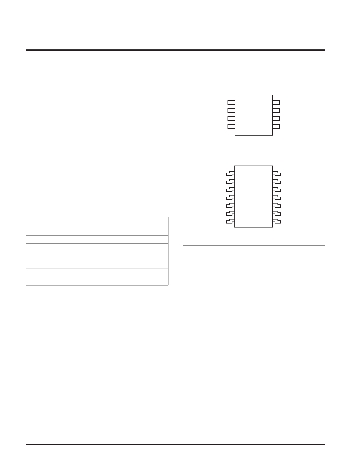
PIN CONFIGURATION
DIP/SOIC
A0
A1
A2
VSS
1
8
2
7
X24C16
3
6
4
5
VCC
TEST
SCL
SDA
3840 FHD F02
NC
A0
A1
NC
A2
VSS
NC
SOIC
1
14
2
13
3
12
4 X24C16 11
5
10
6
9
7
8
NC
VCC
TEST
NC
SCL
SDA
NC
3840 FHD F03
2
Share Link: 