W133 데이터 시트보기 (PDF) - Cypress Semiconductor
부품명
상세내역
일치하는 목록
W133 Datasheet PDF : 12 Pages
| |||
PRELIMINARY
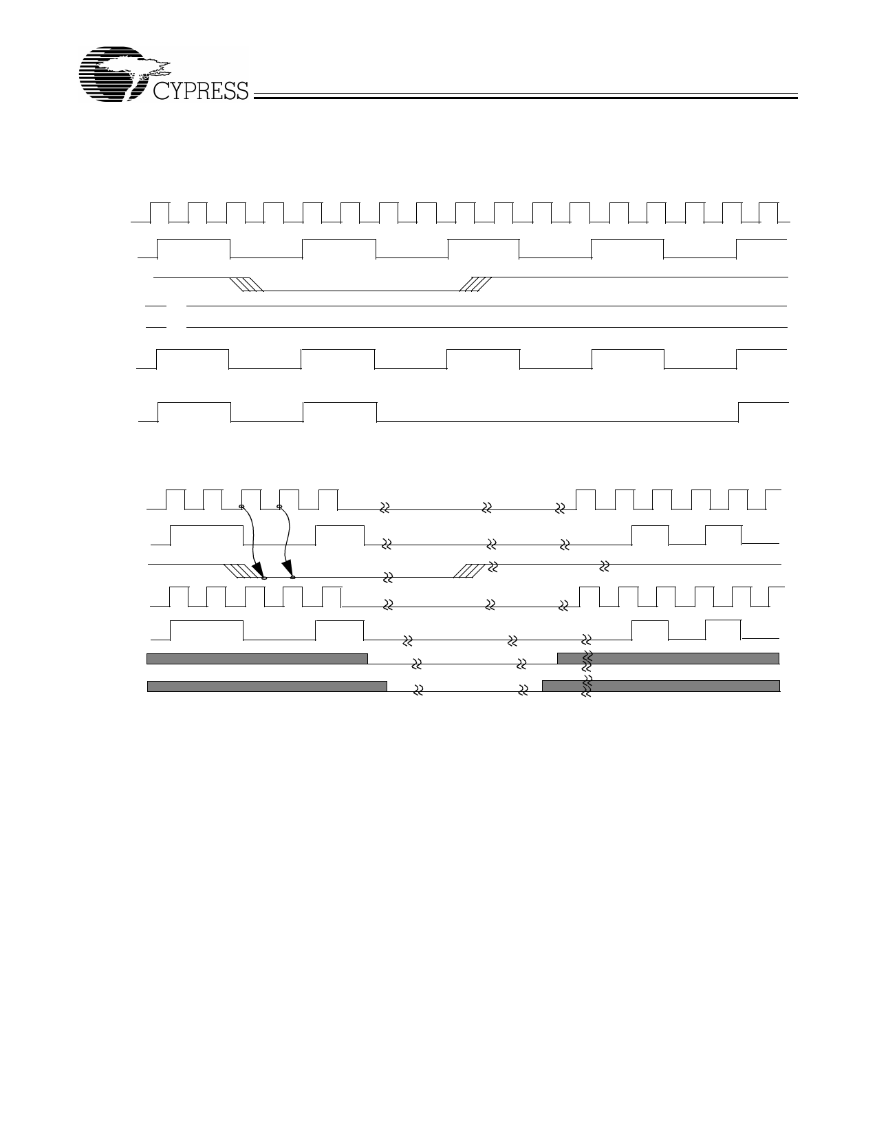
Timing Diagrams (continued)
PCI_STOP# Timing Diagram[17, 18, 22, 23, 24, 25]
CPU
PCI
(internal)
PCI_STOP#
CPU_STOP#
HI
PWRDWN#
HI
PCI_F
(external)
PCI
(external)
PWRDWN# Timing Diagram[17, 22, 26, 27]
CPU
(internal)
PCI
(internal)
PWRDWN#
CPU
(external)
PCI
(external)
VCO
Crystal
Notes:
23. PCI_STOP# signal is an input signal that must be made synchronous to PCI_F output.
24. All other clocks continue to run undisturbed.
25. PWRDWN# and CPU_STOP# are shown in a HIGH state.
26. The internal label means inside the chip and is a reference only. This in fact may not be the way that the control is designed.
27. PWRDWN is an asynchronous input and metastable conditions could exist. This signal is required to be synchronized.
28. The shaded sections on the VCO and the Crystal signals indicate an active clock.
W133
6
Share Link: 