MC74HC4017D 데이터 시트보기 (PDF) - Motorola => Freescale
부품명
상세내역
일치하는 목록
MC74HC4017D Datasheet PDF : 9 Pages
| |||
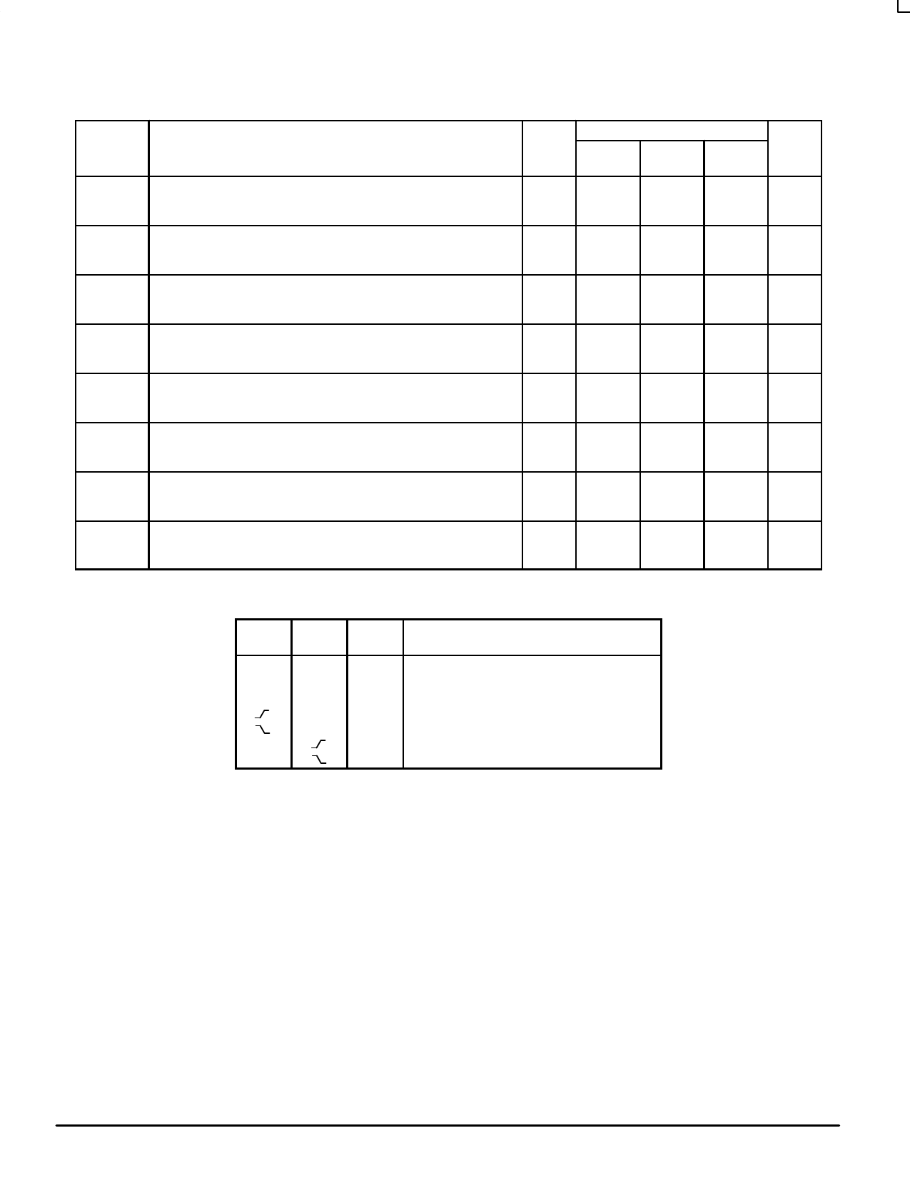
MC74HC4017
ÎÎÎÎÎÎÎÎÎÎÎÎÎÎÎÎÎÎÎÎÎÎÎÎÎÎÎÎÎÎÎÎÎÎÎÎÎÎÎÎÎÎÎÎÎÎÎÎÎÎÎÎÎÎÎÎÎÎÎÎÎÎÎÎÎÎ TIMING REQUIREMENTS (Input tr = tf = 6 ns)t
ÎÎÎÎÎÎÎÎÎÎÎÎÎÎÎÎÎÎÎÎÎÎÎÎÎÎÎÎÎÎÎÎÎ Guaranteed Limit
ÎÎÎÎÎÎÎÎÎÎÎÎÎÎÎÎÎÎÎÎÎÎÎÎÎÎÎÎÎÎÎÎÎÎÎÎÎÎÎÎÎÎÎÎÎÎÎÎÎÎÎÎÎÎÎÎÎÎÎÎÎÎÎÎÎÎ Symbol
Parameter
VCC
V
v v – 55 to
25_C
85_C
125_C Unit
tsu
Minimum Setup Time, Clock Enable to Clock
ÎÎÎÎÎÎÎÎÎÎÎÎÎÎÎÎÎÎÎÎÎÎÎÎÎÎÎÎÎÎÎÎÎÎÎÎÎÎÎÎÎÎÎÎÎÎÎÎÎÎÎÎÎÎÎÎÎÎÎÎÎÎÎÎÎÎ (Figure 6)
2.0
50
65
75
ns
4.5
10
13
15
6.0
9
11
13
ÎÎÎÎÎÎÎÎÎÎÎÎÎÎÎÎÎÎÎÎÎÎÎÎÎÎÎÎÎÎÎÎÎ tsu
Minimum Setup Time, Clock Enable to Clock (Inhibit Count)
ÎÎÎÎÎÎÎÎÎÎÎÎÎÎÎÎÎÎÎÎÎÎÎÎÎÎÎÎÎÎÎÎÎ (Figure 6)
2.0
50
65
75
ns
4.5
10
13
15
6.0
9
11
13
ÎÎÎÎÎÎÎÎÎÎÎÎÎÎÎÎÎÎÎÎÎÎÎÎÎÎÎÎÎÎÎÎÎ th
Minimum Hold Time, Clock to Clock Enable
ÎÎÎÎÎÎÎÎÎÎÎÎÎÎÎÎÎÎÎÎÎÎÎÎÎÎÎÎÎÎÎÎÎ (Figure 6)
2.0
50
65
75
ns
4.5
10
13
15
6.0
9
11
13
ÎÎÎÎÎÎÎÎÎÎÎÎÎÎÎÎÎÎÎÎÎÎÎÎÎÎÎÎÎÎÎÎÎ trec
Minimum Recovery Time, Reset to Clock
ÎÎÎÎÎÎÎÎÎÎÎÎÎÎÎÎÎÎÎÎÎÎÎÎÎÎÎÎÎÎÎÎÎ (Figure 7)
2.0
100
125
150
ns
4.5
20
25
30
6.0
17
21
26
ÎÎÎÎÎÎÎÎÎÎÎÎÎÎÎÎÎÎÎÎÎÎÎÎÎÎÎÎÎÎÎÎÎ tw
Minimum Pulse Width, Clock Input
ÎÎÎÎÎÎÎÎÎÎÎÎÎÎÎÎÎÎÎÎÎÎÎÎÎÎÎÎÎÎÎÎÎ (Figure 2)
2.0
80
4.5
16
6.0
14
100
120
ns
20
24
17
20
ÎÎÎÎÎÎÎÎÎÎÎÎÎÎÎÎÎÎÎÎÎÎÎÎÎÎÎÎÎÎÎÎÎ tw
Minimum Pulse Width, Reset Input
ÎÎÎÎÎÎÎÎÎÎÎÎÎÎÎÎÎÎÎÎÎÎÎÎÎÎÎÎÎÎÎÎÎ (Figure 3)
2.0
80
4.5
16
6.0
14
100
120
ns
20
24
17
20
ÎÎÎÎÎÎÎÎÎÎÎÎÎÎÎÎÎÎÎÎÎÎÎÎÎÎÎÎÎÎÎÎÎ tw
Minimum Pulse Width, Clock Enable Input
ÎÎÎÎÎÎÎÎÎÎÎÎÎÎÎÎÎÎÎÎÎÎÎÎÎÎÎÎÎÎÎÎÎÎÎÎÎÎÎÎÎÎÎÎÎÎÎÎÎÎÎÎÎÎÎÎÎÎÎÎÎÎÎÎÎÎ (Figure 4)
2.0
80
4.5
16
6.0
14
100
120
ns
20
24
17
20
ÎÎÎÎÎÎÎÎÎÎÎÎÎÎÎÎÎÎÎÎÎÎÎÎÎÎÎÎÎÎÎÎÎ tr, tf
Maximum Input Rise and Fall Times
ÎÎÎÎÎÎÎÎÎÎÎÎÎÎÎÎÎÎÎÎÎÎÎÎÎÎÎÎÎÎÎÎÎ (Figure 1)
2.0
1000
1000
1000
ns
4.5
500
500
500
6.0
400
400
400
ÎÎÎÎÎÎÎÎÎÎÎÎÎÎÎÎÎÎÎÎÎÎÎÎÎÎÎÎÎÎÎÎÎ NOTE: Information on typical parametric values can be found in Chapter 2 of the Motorola High–Speed CMOS Data Book (DL129/D).
FUNCTION TABLE
Clock
Clock Enable Reset
Output State*
L
X
L
no change
X
H
L
no change
X
X
H
reset counter, Q0 = H, Q1 – Q9 = L, C0 = H
L
L
advance to next state
X
L
X
L
no change
no change
H
L
advance to next state
X = Don’t care
* Carry Out = H for Q0, Q1, Q2, Q3, or Q4 = H; Carry Out = L otherwise.
PIN DESCRIPTIONS
INPUTS
Clock (Pin 14)
Counter clock input. While Clock Enable is low, a low–to–
high transition on this input advances the counter to its next
state.
Reset (Pin 15)
Asynchronous counter reset input. A high level at this input
initializes the counter and forces Q0 and Carry Out to a high,
Q1–Q9 are forced to a low level.
Clock Enable (Pin 13)
Active–low clock enable input. A low level on this input al-
lows the device to count. A high level on this input inhibits the
counting operation. This input may also be used as a
negative–edge clock input. using Clock (Pin 14) as an
active–high enable pin.
OUTPUTS
Q0 – Q9 (Pins 3, 2, 4, 7, 10, 1, 5, 6, 9, 11)
Decoded decade counter outputs. Each of these outputs is
high for one clock period only.
Carry Out (Pin 12)
Cascading output pin. This output is used either as a cas-
cading output or a symmetrical divide–by–ten output. This
output goes low when a count of five is reached and high
when the counter advances to zero or when reset. When the
counters are cascaded this output provides a rising–edge
signal for the clock input of the next counter stage.
MOTOROLA
4
High–Speed CMOS Logic Data
DL129 — Rev 6
Share Link: 