V6340PSP3B 데이터 시트보기 (PDF) - EM Microelectronic - MARIN SA
부품명
상세내역
일치하는 목록
V6340PSP3B Datasheet PDF : 8 Pages
| |||
R
V6340
Absolute Maximum Ratings
Parameter
Voltage at VDD to VSS
Minimum voltage at RES or
RES
Maximum voltage at RES or
RES
Storage Temperature Range
Symbol
VDD
Vmin
Conditions
-0.3V to +8V
VSS – 0.3V
Vmax
TSTO
VDD + 0.3V
-65°C to +150°C
Table 1
Stresses above these listed maximum ratings may cause
permanent damages to the device. Exposure beyond
specified operating conditions may affect device reliability or
cause malfunction.
Handling Procedures
This device has built-in protection against high static
voltages or electric fields; however, it is advised that normal
precautions be taken as for any other CMOS component.
Unless otherwise specified, proper operation can only occur
when all terminal voltages are kept within the voltage range.
Operating Conditions
Parameter
Symbol Min Max Unit
Operating Temperature 1) TA -40 +125 °C
Positive Supply Voltage 2) VDD
1
5.5
V
Table 2
1)The maximum operating temperature is confirmed by
sampling at initial device qualification. In production, all
devices are tested at +25°C
2) VDD = 1V guaranteed at +25°C (see Fig. 14 for more
information)
Electrical Characteristics
TA = +25°C, unless otherwise specified
Parameter
Supply current
Threshold voltage
Threshold hysteresis
RES Output Low Level
RES Output High Level
Output leakage current1)
Symbol
IDD
VTH
VTH
VTH
VHYS
VOL
VOL
VOL
VOL
VOH
VOH
VOH
VOH
ILEAK
Only for version B, H and N
Parameter
Supply current
Threshold voltage
Threshold hysteresis
Symbol
IDD
VTH
VHYS
Test Conditions
VDD = 5V, output open
C, I, O
D, J, P
F, L, R
VDD = 1.6V, IOL = 1mA
VDD = 2.5V, IOL = 2mA
VDD = 3.5V, IOL = 3mA
VDD = 5V, IOL = 4mA
VDD = 1.6V, IOH = -1mA
VDD = 2.5V, IOH = -1.5mA
VDD = 3.5V, IOH = -2.5mA
VDD = 5V, IOH = -3.5mA
VDD = 5V
Test Conditions
VDD = 5V, output open
B, H, N
Min.
2.94
3.62
4.27
1.25
2.2
3.15
4.65
Typ.
38
3.02
3.72
4.39
5
200
195
198
185
1.36
2.3
3.27
4.76
0.005
Max.
50
3.10
3.82
4.51
270
250
250
250
1
Min.
2.56
Typ.
19
2.65
32
Max.
31
2.74
1) Only for Open drain versions
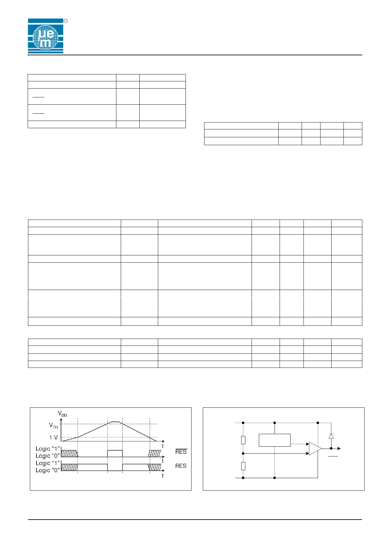
Timing Waveform
Block Diagram
Unit
µA
V
V
V
mV
mV
mV
mV
mV
V
V
V
V
µA
Unit
µA
V
mV
Table 3
VDD
Voltage
Reference
-
+
RES or
RES
VSS
Fig.3
Fig.4
Copyright © 2005, EM Microelectronic-Marin SA
2
03/06 – rev.K
www.emmicroelectronic.com
Share Link: 