UPD72001C-11 데이터 시트보기 (PDF) - NEC => Renesas Technology
부품명
상세내역
일치하는 목록
UPD72001C-11 Datasheet PDF : 40 Pages
| |||
µPD72001-11, 72001-A8
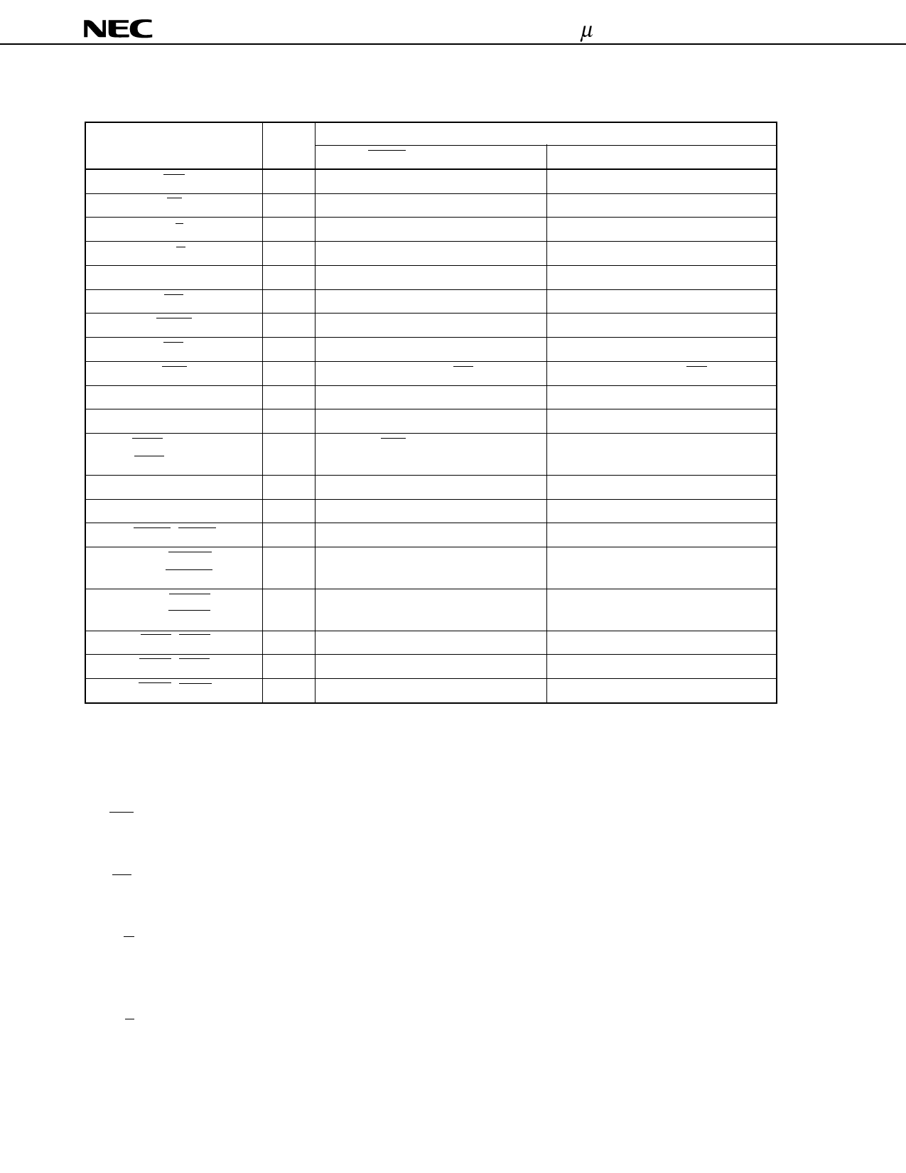
Table 1-1. Pin Status at Reset
Pin Name
I/O
WR
I
RD
I
B/A
I
C/D
I
D7 to D0
I/O
INT
O
INTAK
I
PRI
I
PRO
O
DRQTXA
O
DRQRXA
O
DTRA/DRQTXB,
O
DTRB/DRQRXB
TXDA, TXDB
O
RXDA, RXDB
I
TRXCA, TRXCB
I/O
XI1A/STRXCA
I
XI1B/STRXCB
XI2A/SYNCA
I/O
XI2B/SYNCB
RTSA, RTSB
O
CTSA, CTSB
I
DCDA, DCDB
I
RESET (system reset)
–
–
–
–
–
High impedance
–
–
Depends on PRI
“L”
“L”
DTR function, “H”
Pin Status
Channel reset
–
–
–
–
–
High impedance
–
–
Depends on PRI
“L”
“L”
Retains current status
“H”
–
Input status
–
“H”
–
Retains current status
–
Input status
Retains current status
“H”
“H”
–
–
–
–
– : Undefined
(4) CLK (System Clock) ... Input
This pin inputs the system clock. The input frequency must be five times that of the data transfer rate or higher.
(5) WR (Write) ... Input
This pin inputs a write control signal for control words and transmit data. This pin is active-low.
(6) RD (Read) ... Input
This pin inputs a read control signal for status and receive data. This pin is active-low.
(7) B/A (Channel B/Channel A) ... Input
This pin inputs a signal to select a channel to be accessed when data is written or read. When this pin is “L”,
channel A is selected; when it is “H”, channel B is selected.
(8) C/D (Control/Data) ... Input
This pin inputs a signal that determines the type of the data on the data bus when the data is written or read.
8
Share Link: 