UM61512A 데이터 시트보기 (PDF) - UMC Corporation
부품명
상세내역
일치하는 목록
UM61512A Datasheet PDF : 16 Pages
| |||
UM61512A
AC Test Conditions
Input Pulse Levels
Input Rise and Fall Time
Input and Output Timing Reference Levels
Output Load
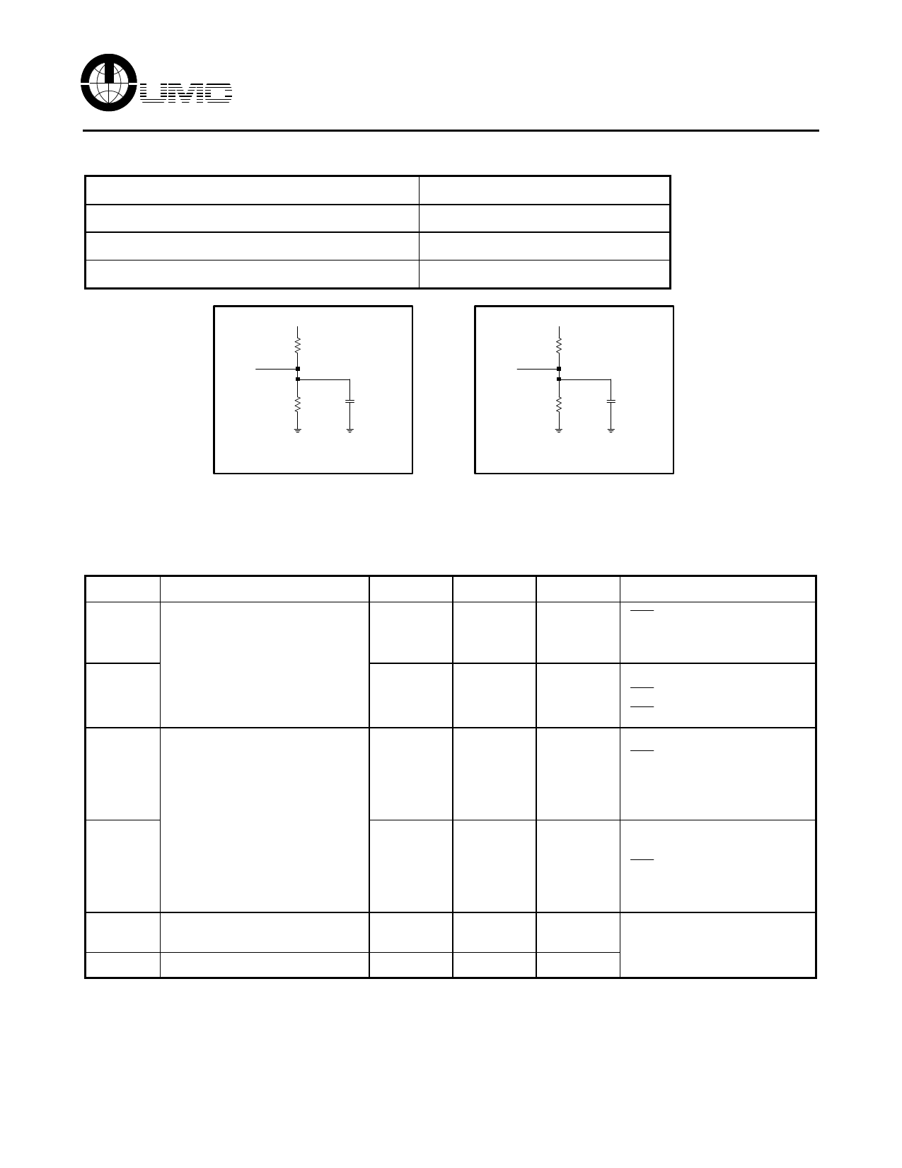
+5V
480Ω
I/O
255Ω
30pF*
* Including scope and jig.
Figure 1.Output Load
Data Retention Characteristics (TA = 0°C to 70°C)
Symbol
VDR1
Parameter
Min.
3
VCC for Data Retention
VDR2
3
ICCDR1
-
Data Retention Current
ICCDR2
-
tCDR
Chip Disable to Data Retention
0
Time
tR
Operation Recovery Time
5
0V to 3.0V
5 ns
1.5V
See Figures 1 and 2
+5V
480Ω
I/O
255Ω
5pF*
* Including scope and jig.
Figure 2. Output Load for tCLZ1,
tCLZ2, tOLZ, tCHZ1, tCHZ2,
tOHZ, tWHZ, and tOW
Max.
5.25
5.25
5
5
-
-
Unit
V
V
mA
mA
ns
ms
Conditions
CE1 ≥ VCC - 0.2V
CE2 ≥ VCC - 0.2V or
CE2 ≤ 0.2V
CE2 ≤ 0.2V
CE1 ≥ VCC - 0.2V or
CE1 ≤ 0.2V
VCC = 3.0V
CE1 ≥ VCC - 0.2V
CE2 ≥ VCC - 0.2V
VIN ≥ VCC - 0.2V or
VIN ≤ 0.2V
VCC = 3.0V
CE2 ≤ 0.2V
CE1 ≤ 0.2V
VIN ≥ VCC - 0.2V or
VIN ≤ 0.2V
See Retention Waveform
10
Share Link: 