HT7660(1999) 데이터 시트보기 (PDF) - Holtek Semiconductor
부품명
상세내역
일치하는 목록
HT7660 Datasheet PDF : 9 Pages
| |||
HT7660
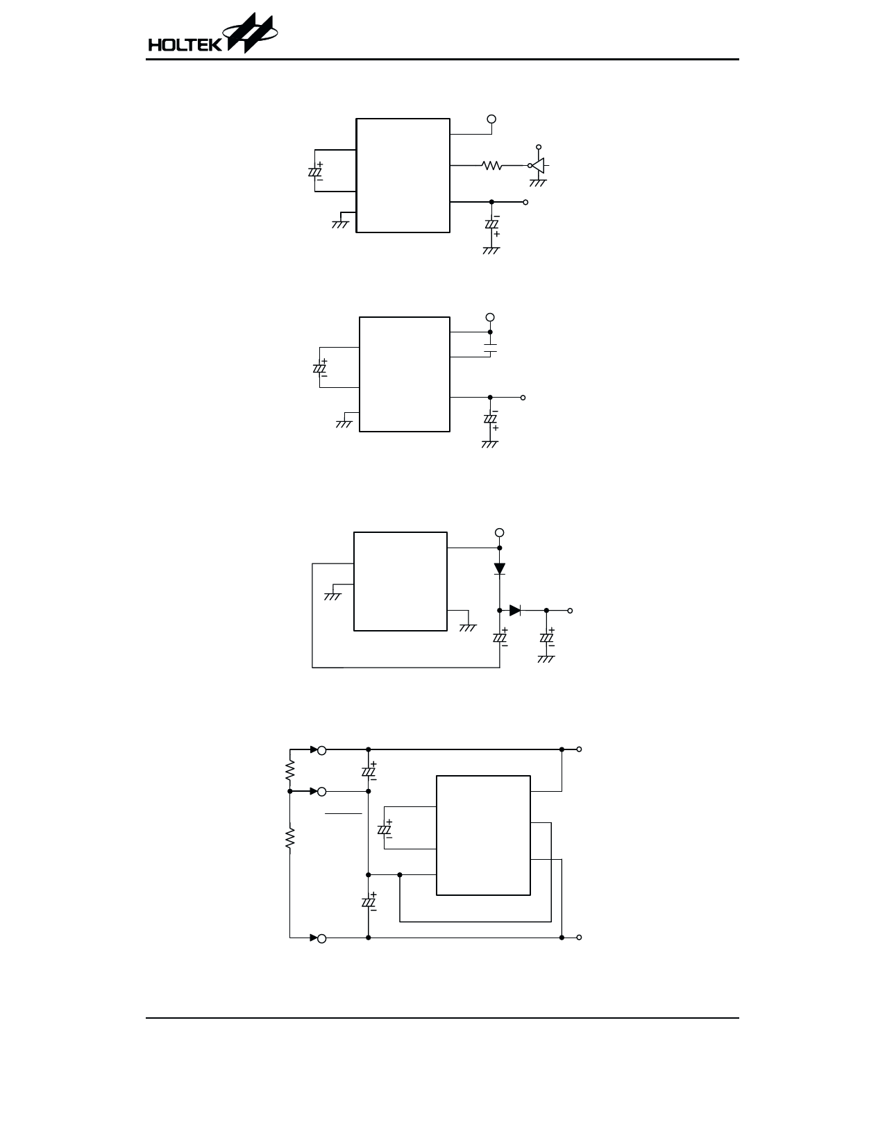
Functional Description
HT7660 needs only two external polarized elec-
trolytic capacitors to complete a negative volt-
age converter.
HT7660 has four MOS power switches: S1, S2,
S3 and S4. For the first half cycle, when S2 and
S4 are open, Capacitor C1 is charged to a volt-
age VDD through S1 and S3. During the second
half cycle, when S1 and S3 are open, the charge
on Capacitor C1 is shifted to Capacitor C2
through S2 and S4. Thereby, the voltage across
Capacitor C2 is VDD. Because the positive ter-
minal of C2 is connected to VSS, we get a -VDD
voltage at VOUT pin.
For high voltage operation, the LV pin is left
floating to enable the voltage regulator. This
can reduce the current consumption of the RC
oscillator, and thus get a fixed switching fre-
quency Fosc with high voltage range. For low
voltage operation, the LV pin is connected to
VSS to bypass the voltage regulator of which in-
herent voltage drop can degrade the operation
at low voltages.
A capacitor may be connected between VDD and
pin OSC to lower the switching Fosc, and an ex-
ternal clock may be added to replace the
built-in RC oscillator.
V DD
S1
CAP+ S2
C1
V SS
S3
S4
CAP-
V SS
C2
V O UT= - V DD
The operating mode of HT7660
4
November 30, 1999
Share Link: 