AK93C55A 데이터 시트보기 (PDF) - Asahi Kasei Microdevices
부품명
상세내역
일치하는 목록
AK93C55A Datasheet PDF : 15 Pages
| |||
ASAHI KASEI
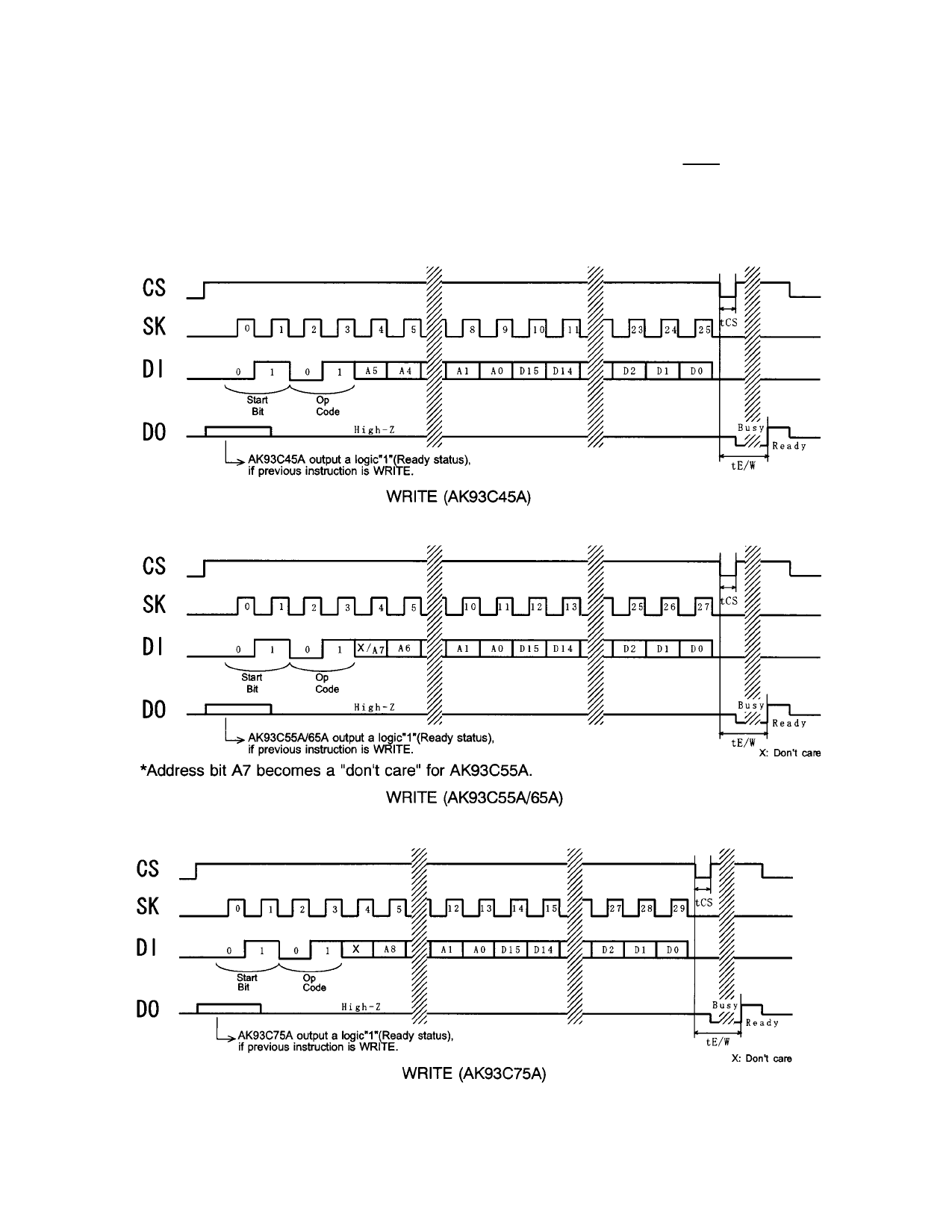
[AK93C45A/55A/65A/75A]
Write
The write instruction is followed by 16 bits of data to be written into the specified address. After the last bit of
data is put on the DI pin, the CS pin must be brought low before the next rising edge of the SK clock. This
falling edge of the CS initiates the self-timed programming cycle. The DO indicates the Busy/Ready status of
the chip if the CS is brought high after a minimum of 250ns (Tcs). DO=logical "0" indicates that programming
is still in progress. DO=logical "1" indicates that the register at the address specified in the instruction has
been written with the new data pattern contained in the instruction and the part is ready for a next instruction.
DAM01E-01
-6-
1999/10
Share Link: 