CDP1883 데이터 시트보기 (PDF) - Intersil
부품명
상세내역
일치하는 목록
CDP1883 Datasheet PDF : 6 Pages
| |||
CDP1883, CDP1883C
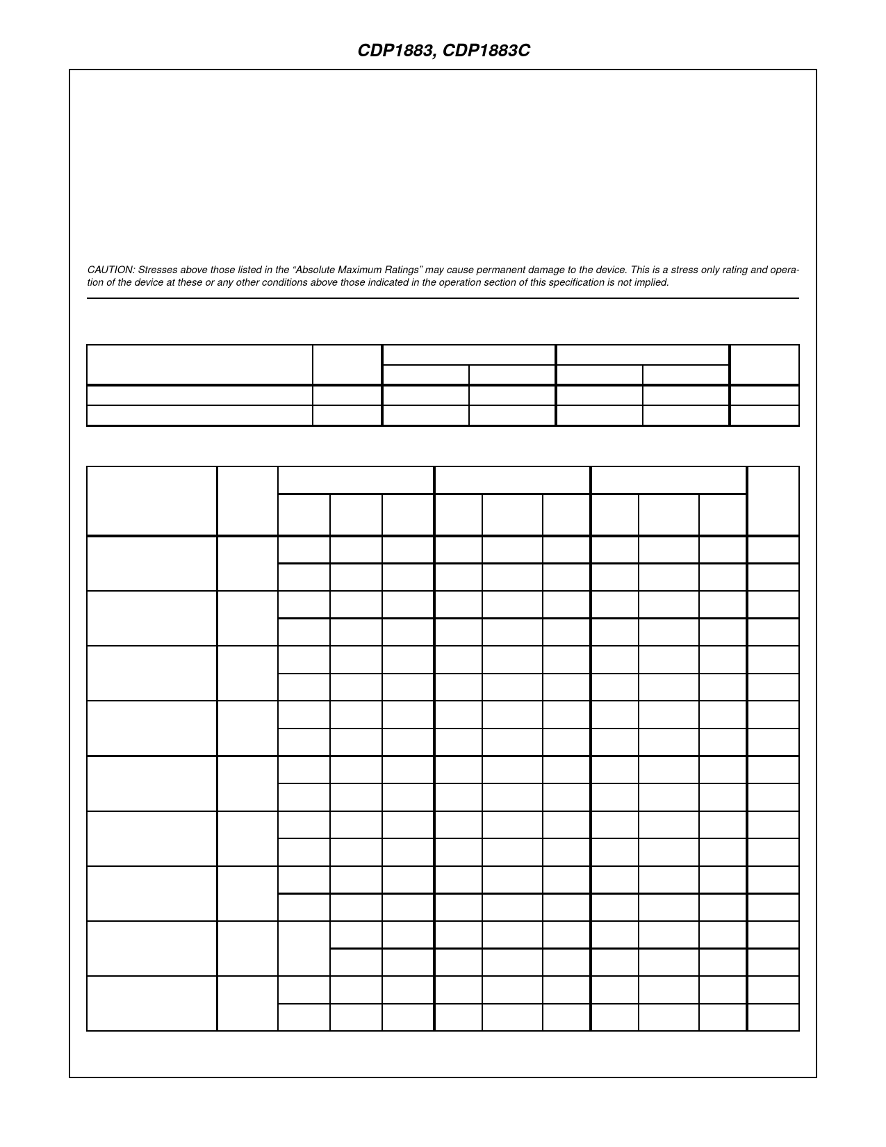
Absolute Maximum Ratings
Thermal Information
DC Supply Voltage Range, (VDD)
(All Voltages Referenced to VSS Terminal)
CDP1883 . . . . . . . . . . . . . . . . . . . . . . . . . . . . . . . . -0.5V to +11V
CDP1883C. . . . . . . . . . . . . . . . . . . . . . . . . . . . . . . . -0.5V to +7V
Input Voltage Range, All Inputs . . . . . . . . . . . . . -0.5V to VDD +0.5V
DC Input Current, Any One Input. . . . . . . . . . . . . . . . . . . . . . . . .±10mA
Thermal Resistance (Typical)
θJA (oC/W)
PDIP Package . . . . . . . . . . . . . . . . . . . . . . . . . . . . .
80
Device Dissipation Per Output Transistor
TA = Full Package Temperature Range . . . . . . . . . . . . . . . 100mW
Operating Temperature
Package Type E . . . .
Range
......
(TA)
....
.
.
.
.
.
.
.
.
.
.
.
.
.-40oC
to
+85oC
Storage Temperature Range (TSTG). . . . . . . . . . . .-65oC to +150oC
Lead Temperature (During Soldering)
At distance 1/16 ±1/32 In. (1.59 ± 0.79mm)
from case for 10s max . . . . . . . . . . . . . . . . . . . . . . . . . . . . +265oC
CAUTION: Stresses above those listed in the “Absolute Maximum Ratings” may cause permanent damage to the device. This is a stress only rating and opera-
tion of the device at these or any other conditions above those indicated in the operation section of this specification is not implied.
Recommended Operating Conditions At TA = Full Package Temperature Range. For maximum reliability, operating conditions
should be selected so that operation is always within the following ranges:
CDP1883
CDP1883C
PARAMETER
SYMBOL
MIN
MAX
MIN
MAX
UNITS
DC Operating Voltage Range
Input Voltage Range
4
10.5
4
6.5
V
VSS
VDD
VSS
VDD
V
Static Electrical Specifications At TA = -40oC to +85oC, VDD ± 5%, Except as Noted:
CONDITIONS
CDP1883
CDP1883C
PARAMETER
VO
SYMBOL (V)
VIN
VDD
(NOTE 1)
(NOTE 1)
(V)
(V)
MIN
TYP
MAX MIN
TYP
MAX UNITS
Quiescent Device
Current
IDD
-
0, 5
5
-
1
10
-
-
0, 10
10
-
10
100
-
5
50
µA
-
-
µA
Output Low Drive
(Sink) Current
IOL
0.4
0, 5
5
1.6
3.2
0.5
0, 10
10
3.2
6.4
-
1.6
3.2
-
-
-
-
mA
-
mA
Output High Drive
(Source) Current
IOH
4.6
0, 5
5
-1.15
-2.3
9.5
0, 10
10
-2.3
-4.6
-
-1.15
-2.3
-
-
-
-
mA
-
mA
Output Voltage
Low-Level (Note 2)
VOL
-
0, 5
5
-
-
0, 10
10
-
0
0.1
-
0
0.1
-
0
0.1
V
-
-
V
Output Voltage
High-Level (Note 2)
VOH
-
0, 5
5
4.9
5
-
0, 10
10
9.9
10
-
4.9
5
-
-
-
-
V
-
V
Input Low Voltage
VIL
0.5, 4.5
-
5
-
0.5, 9.5
-
10
-
-
1.5
-
-
3
-
-
1.5
V
-
-
V
Input High Voltage
VIH
0.5, 4.5
-
5
3.5
-
0.5, 9.5
-
10
7
-
-
3.5
-
-
-
-
-
V
-
V
Input Leakage Current
IIN
Any
0, 5
5
-
Input
0, 10
10
-
-
±1
-
-
±2
-
-
±1
µA
-
-
µA
Operating Current
(Note 3)
IDD1
0, 5
0, 5
5
-
0, 10 0, 10
10
-
-
2
-
-
4
-
-
2
mA
-
-
mA
4-130
Share Link: 