TDA1180 데이터 시트보기 (PDF) - STMicroelectronics
부품명
상세내역
일치하는 목록
TDA1180 Datasheet PDF : 12 Pages
| |||

TDA1180P
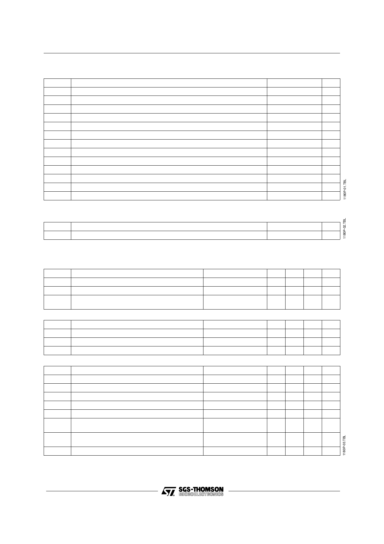
ABSOLUTE MAXIMUM RATINGS
Symbol
VS
V2
V4
V8
V9
V11
I2
I3
I6
I7
I10
Ptot
Tstg , Tj
Parameter
Supply voltage (Pin 1)
Voltage at Pin 2
Voltage at Pin 4
Voltage at Pin 8
Voltage at Pin 9
Voltage at Pin 11
Pin 2 peak current
Pin 3 peak current
Pin 6 current
Pin 7 current
Pin 10 current
Total power dissipation at Tamb ≤ 70oC
Storage and junction temperature
Value
15
18
VS
- 6 , VS
±6
VS
1
0.5
30
20
30
1
- 40 , + 150
Unit
V
V
V
V
A
A
mA
mA
mA
W
oC
THERMAL DATA
Symbol
Parameter
Rth (j-a) Thermal Resistance Junction-Ambient
Value
Unit
Max
80
oC/W
ELECTRICAL CHARACTERISTICS
(refer to the test circuit, VS = 12V, TA = 25oC, unless otherwise specified)
Symbol
VS
IS
VS
Parameter
Supply voltage range
Supply current
Supply voltage at which the output pulses
(at pin 2 and 3) are switched off
Test conditions
I3 = 0
HORIZONTAL SYNC. SEPARATOR
VI
Peak to peak input signal
V8
Input switching voltage
I8
Input switching current
I8
Leakage current
VERTICAL SYNC. SEPARATOR
I8 = 80 µA
V8 = 1.4V
V8 = -5V
VI
Peak to Peak Input Signal
V9
Input Switching Voltage
I9= 80µA
I9
Input Switching Current
V9 = 1.4V
I9
Leakage Current
V9 = -5V
V10 Vertical Sync. Pulse Output Voltage
No Load Pin10
R10 Output Resistance
tLV
Delay between Leading Edge of Input and Output
Signals
tLV
Delay between Trailing Edge of Input and Output
Signals
tV
Vertical Sync Pulse Duration
Min. Typ. Max. Unit
9.5 12 13.2 V
42 52 mA
4
V
1
3
6
V
1.5
V
10
µA
1 µA
1
3
6
V
1.5
V
5
µA
1 µA
11
V
10
kΩ
17
µs
50
µs
190
µs
3/12