TC1262 데이터 시트보기 (PDF) - Microchip Technology
부품명
상세내역
일치하는 목록
TC1262 Datasheet PDF : 12 Pages
| |||
2.0 PIN DESCRIPTIONS
The descriptions of the pins are listed in Table 2-1.
TABLE 2-1: PIN FUNCTION TABLE
Pin No.
(3-Pin SOT-223)
(3-Pin TO-220)
(3-Pin DDPAK)
1
2
3
Symbol
VIN
GND
VOUT
Unregulated supply input.
Ground terminal.
Regulated voltage output.
3.0 DETAILED DESCRIPTION
The TC1262 is a precision, fixed output LDO. Unlike
bipolar regulators, the TC1262’s supply current does
not increase with load current. In addition, VOUT
remains stable and within regulation over the entire
0mA to ILOADMAX load current range (an important
consideration in RTC and CMOS RAM battery back-up
applications).
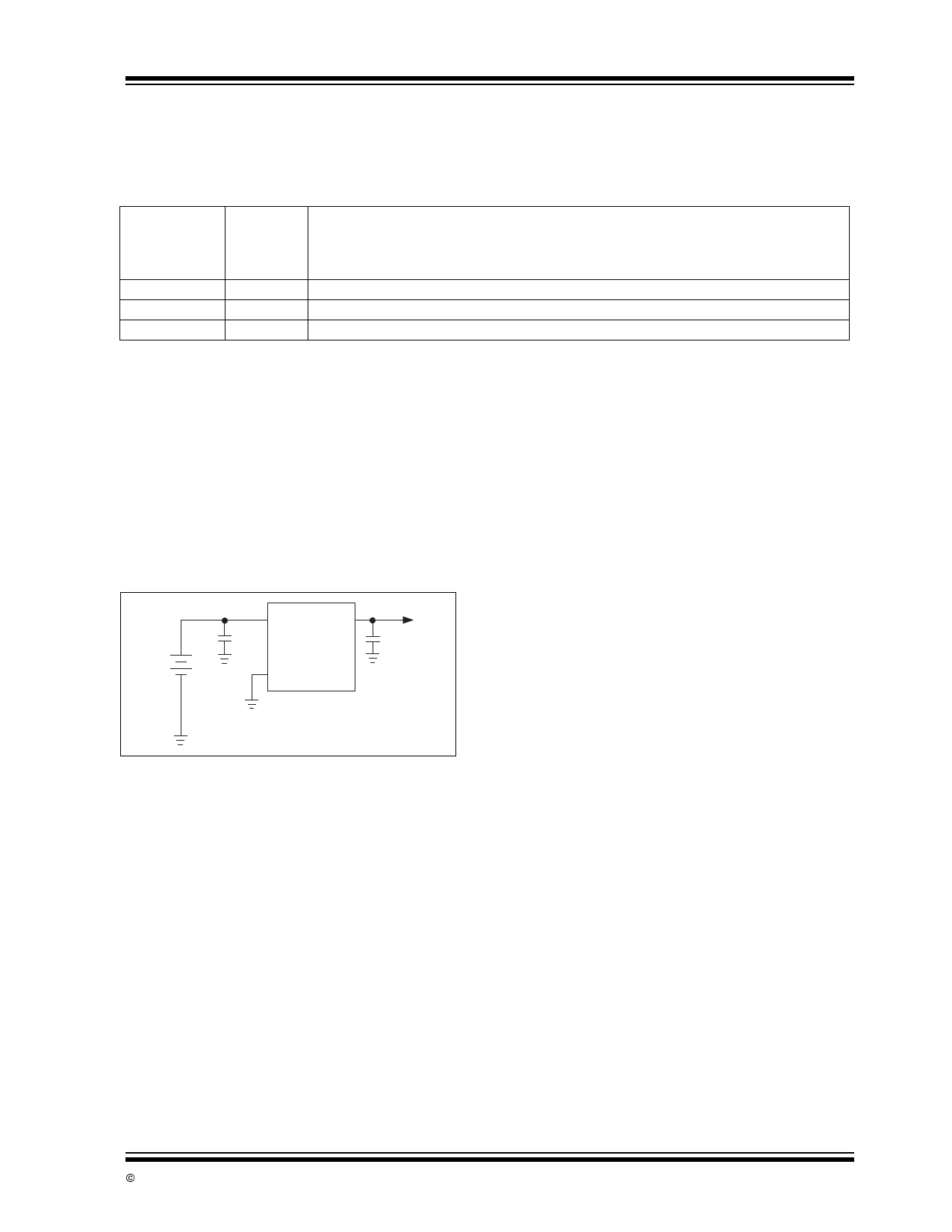
Figure 3-1 shows a typical application circuit.
FIGURE 3-1:
TYPICAL APPLICATION
CIRCUIT
Battery
+
+
C1
1µF
VIN
VOUT +
TC1262
C2
1µF
VOUT
–
GND
TC1262
Description
3.1 Output Capacitor
A 1µF (min) capacitor from VOUT to ground is required.
The output capacitor should have an effective series
resistance greater than 0.1Ω and less than 5Ω, and a
resonant frequency above 1MHz. A 1µF capacitor
should be connected from VIN to GND if there is more
than 10 inches of wire between the regulator and the
AC filter capacitor, or if a battery is used as the power
source. Aluminum electrolytic or tantalum capacitor
types can be used. (Since many aluminum electrolytic
capacitors freeze at approximately -30°C, solid
tantalums are recommended for applications operating
below -25°C.) When operating from sources other than
batteries, supply-noise rejection and transient
response can be improved by increasing the value of
the input and output capacitors and employing passive
filtering techniques.
© 2002 Microchip Technology Inc.
DS21373B-page 3
Share Link: 