TA2145AF 데이터 시트보기 (PDF) - Toshiba
부품명
상세내역
일치하는 목록
TA2145AF Datasheet PDF : 16 Pages
| |||
TA2145AF
Application Note
· VCC and GND
This IC has two VCC terminals and three GND terminals. Pattern layout should be designed carefully to
reduce the common impedance.
· VCC
VCC (pin 17) ----------------- Preamplifier stage and power amplifier stage.
GVN VCC (pin 16) --------- Motor governor stage.
· GND
PRE GND (pin 1)------------Preamplifier stage, and power amplifier stage except for the power drive stage.
PW GND (pin 11) -----------Power drive stage of power amplifier.
GVN GND (pin 12) ---------Motor governor stage.
· VREF
It is necessary to stabilize the VREF circuit, because the internal circuit operate on this reference.
· RF IN
As this terminal is an input terminal of the ripple filter, it cannot supply a power supply to other ICs etc.
· Preamplifier
Input signal should be applied to VREF standard, otherwise pop noise become bigger when VCC is turned on
and off.
· Power amplifier
It is necessary to insert the coupling capacitor through the PW IN terminal. In case that DC current or DC
voltage is applied to the PW IN terminal, the internal circuit has unbalance and the power amplifier doesn’t
operate normally.
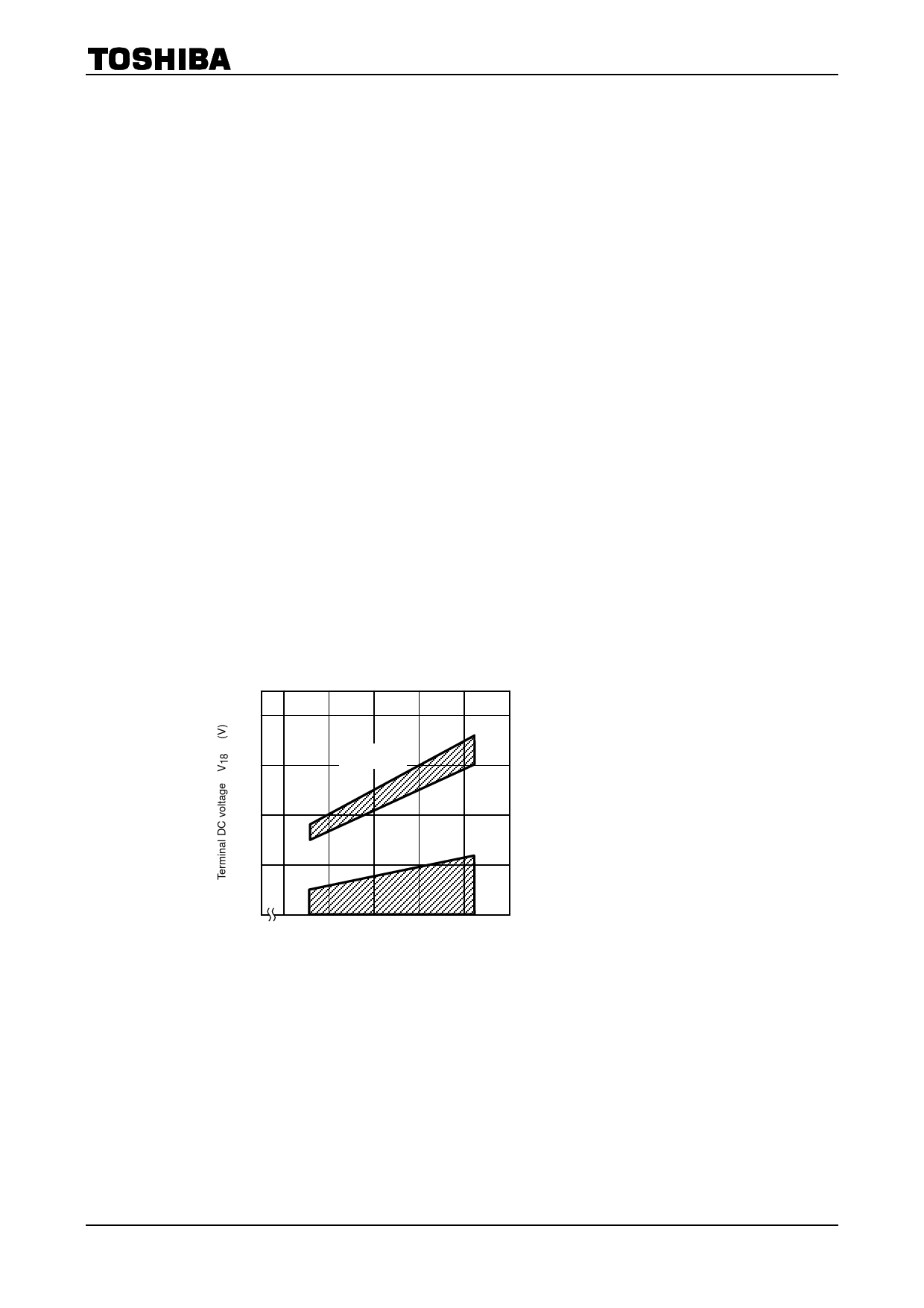
· Operating supply voltage range of motor governor stage
As for the minimum of operating supply voltage range, the motor voltage is 1.8 V.
In case that it is more than 1.8 V, the low voltage performance becomes bad.
· PRE SW sensitivity (Ta = 25°C)
PRE SW
4
3.6 V
“H”
3
PRE AMP: OFF
3.0 V
2
1.8 V
1.5 V
1
0.5 V
1.2 V
0 1.5
2.0
2.5
3.0
3.5
4.0
Supply voltage VCC (V)
6
2002-04-19
Share Link: 