CDP1852 데이터 시트보기 (PDF) - Intersil
부품명
상세내역
일치하는 목록
CDP1852 Datasheet PDF : 9 Pages
| |||
CDP1852, CDP1852C
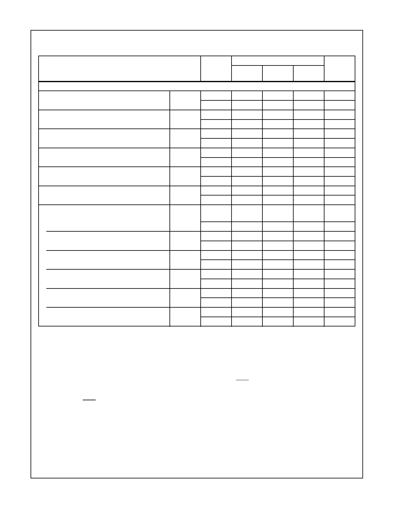
Dynamic Electrical Specifications At TA = -40oC to +85oC, VDD = ±5%, tR, tF = 20ns, VIH = 0.7 VDD, VIL = 0.3 VDD, CL = 100pF,
and 1 TTL Load
PARAMETER
MODE 1- OUTPUT PORT (See Figure 6)
Minimum Clock Pulse Width
Minimum Write Pulse Width
Minimum Clear Pulse Width
LIMITS
VDD
(NOTE 1)
(V)
MIN
TYP
MAX
UNITS
tCLK
5
10
tWW
5
10
tCLR
5
10
-
130
260
ns
-
65
130
ns
-
130
260
ns
-
65
130
ns
-
60
120
ns
-
30
60
ns
Minimum Data Setup Time
Minimum Data Hold Time
Minimum Select-After-Clock Hold Time
Propagation Delay Times, tPLH, tPHL
Clear to Data Out
tDS
5
10
tDH
5
10
tSH
5
10
tRDO
5
10
-
-10
0
ns
-
-5
0
ns
-
75
150
ns
-
35
75
ns
-
-10
0
ns
-
-5
0
ns
-
140
280
ns
-
70
140
ns
Write to Data Out
tWDO
5
10
-
220
440
ns
-
110
220
ns
Data In to Data Out
tDDO
5
10
-
100
200
ns
-
50
100
ns
Clear to SR
Clock to SR
tRSR
5
10
tCSR
5
10
-
120
240
ns
-
60
120
ns
-
120
240
ns
-
60
120
ns
Select to SR
tSSR
5
10
-
120
240
ns
-
60
120
ns
NOTE:
1. Typical values are for TA = 25oC and nominal VDD.
Output Port Mode 1 - Typical Operation
General Operation
Connecting the mode control to VDD configures the
CDP1852 as an output port. The output drivers are always
on in this mode, so any data in the 8-bit register will be
present at the data-out lines when the CDP1852 is selected.
The N line and MRD connections between the CDP1852
and CDP1802 remain the same as in the input mode
configuration, but now the clock input of the CDP1852 is tied
to the TPB output of the CDP1802 and the SR output of the
CDP1852 will be used to signal the peripheral device that
valid data is present on its input lines. The microprocessor
issues an output instruction, and data from the memory is
strobed into the CDP1852 with the TPB pulse. When the
CDP1852 is deselected, the SR output goes high to signal
the peripheral device.
Detailed Operation (See Figure 7)
The CDP1802 issues an output instruction. The NX line goes
high and the MRD line goes low. The memory is accessed
M(R(X)) → BUS and places data on the DATA BUS. This
data are strobed into the 8-bit register of the CDP1852 when
TPB goes high and latched on the TPB’s trailing edge. The
valid data thus appears on the CDP1852 output lines. When
the CDP1802 output instruction cycle is complete, the NX
line goes low and the SR output goes high. SR will remain
high until the trailing edge of the next TPB pulse, when it will
return low.
7
Share Link: 