MAX1759EUB 데이터 시트보기 (PDF) - Maxim Integrated
부품명
상세내역
일치하는 목록
MAX1759EUB Datasheet PDF : 10 Pages
| |||
Buck/Boost Regulating
Charge Pump in µMAX
Capacitor Selection
Optimize the charge-pump circuit for physical size, out-
put current, and output ripple by selecting capacitors
CIN, CX, and COUT. See Table 1 for suggested capacitor
values.
Note that capacitors must have low ESR (≤20mΩ) to
maintain low output ripple. Ceramic capacitors are
recommended. In cost-sensitive applications where high
output current is needed, the output capacitor may be a
combination of a 1µF ceramic in parallel with a 10µF tan-
talum capacitor. The ceramic capacitor’s low ESR will
help keep output ripple within acceptable levels.
Output Voltage Ripple
The MAX1759 proprietary control scheme automatically
chooses between voltage doubling and voltage step-
down to maintain output voltage regulation over various
load currents and VIN to VOUT voltage differentials.
When VIN is lower than VOUT, the charge pump always
operates in voltage-doubler mode. It regulates the output
voltage by modulating the charge delivered by the
transfer capacitor.
When VIN is higher than VOUT, the charge pump oper-
ates in voltage step-down mode, but may revert to volt-
age-doubler mode if necessary to maintain regulation
under load. While operating in step-down mode, the
output voltage ripple is typically much lower than it is in
voltage-doubler mode (see Typical Operating
Characteristics).
Output Current
The MAX1759 is guaranteed to deliver a regulated 3.3V
at 100mA continuous, from a +2.5V input. Peaks up to
200mA are acceptable as long as the current is
≤100mA (RMS).
Applications Information
PC Board Layout
The MAX1759 is a high-frequency switched-capacitor
voltage regulator. For best circuit performance, use a
ground plane and keep CIN, CX, COUT, and feedback
resistors (if used) close to the device. If using external
feedback, keep the feedback node as small as possi-
ble by positioning the feedback resistors very close to
FB. Suggested PC component placement and board
layout are shown in Figures 4a and 4b.
Chip Information
TRANSISTOR COUNT: 1802
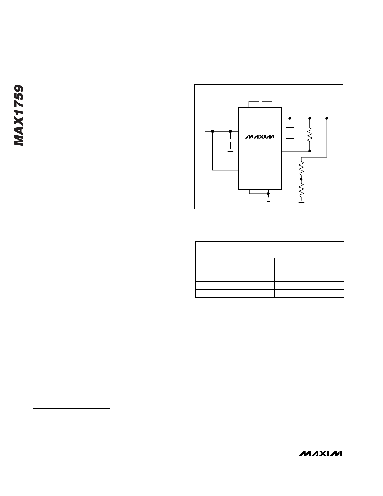
0.33µF
CXN
VIN = 1.6V TO 5.5V
IN
CXP
OUT
10µF
MAX1759
POK
SHDN
GND
FB
PGND
VOUT = 2.5V
10µF
100k
R1
76.8k
R2
75k
Figure 3. Using External Feedback for Regulated 2.5V Output
Table 1. Capacitor Selection
OUTPUT
CURRENT
(mA)
100
100
50
CAPACITOR VALUE
CIN
CX
COUT
(µF)
(µF)
(µF)
10
0.33
10
4.7
0.22
4.7
2.2
0.1
2.2
OUTPUT RIPPLE
(mV)
VIN =
2.5V
40
80
100
VIN =
4.2V
20
60
80
8 _______________________________________________________________________________________
Share Link: 