RF2302 데이터 시트보기 (PDF) - RF Micro Devices
부품명
상세내역
일치하는 목록
RF2302 Datasheet PDF : 8 Pages
| |||
RF2302
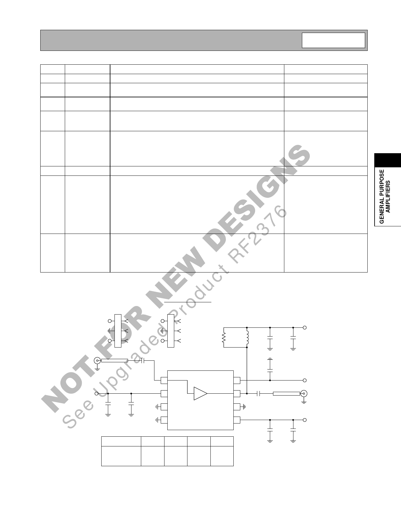
Pin Function Description
Interface Schematic
1
RF IN
RF input pin. This pin is DC coupled and requires a blocking capacitor.
2
VCC
Power supply. This pin is connected to a battery or a regulated supply
and requires a bypass capacitor as close to the pin as possible.
3
GND
Ground connection. Keep traces physically short and connect immedi-
ately to ground plane for best performance.
4
GND
Ground connection. Keep traces physically short and connect immedi-
ately to ground plane for best performance. Use a separate ground via
for this pin.
5
GC
Analog gain control pin. This pin controls the gain of the IC. Minimum
gain occurs at VGC<1V and maximum gain is achieved with VGC=2.2V.
25dB of linear gain control with no variation of input P1dB is available,
and additional attenuation is possible with VGC<1V with input P1dB
variation. Bypass this pin near the device.
4
6
GND
Same as pin 3.
7
RF OUT RF output pin. This pin is DC coupled and requires VCC through a bias
inductor sized accordingly to provide a high pass transformation with a
series capacitor. This LC transformation sets the output load line for the
amplifier. If this amplifier is driving a power amplifier or antenna, no
additional matching is required. However, to improve the output match,
a parallel resistor can be added across the inductor. For 836MHz appli-
cations use a 10nH bias inductor (optional resistor R3=100 ohms) and
2.7pF coupling capacitor. For 1900MHz applications use a 2.7nH bias
inductor (optional resistor R3=150ohms) and 1.0pF coupling capacitor.
8
PD
Power down pin. This pin provides bias for the amplifier. To turn the
amplifier on, this pin should be at 2.8V. Reducing this voltage below
0.5V ensures that the amplifier will draw less than 10µA current from
the supply. Additionally, bias current can be optimized for lower output
power by adjusting this voltage over a 2.7V to 2.9V range from a regu-
lated supply.
Evaluation Board Schematic - 836MHz or 1900MHz
(Download Bill of Materials from www.rfmd.com.)
P1
P2
P1-1 1 GC
P1-1 1 PD
2 GND
2 GND
P1-3 3 VCC P1-3 3 VCC
R3
L1
C3
1 nF
VCC
C12
1 µF
RF IN
50 Ω µstrip
C6
J1
VCC
1
2
C13
C9
1 µF
15 pF
3
2302400-, 401-
C1
22 pF
8
PD
50 Ω µstrip
RF OUT
7
J2
C4
6
4
5
Board
L (836 MHz)
H (1900 MHz)
C6 (pF)
12
3.3
R3 (Ω)
100
150
L1 (nH)
10
2.7
C4 (pF)
2.7
1
GC
C11
C14
1nF
1 µF
Rev A8 010410
4-45
Share Link: 