SMD5962-92324 데이터 시트보기 (PDF) - Cypress Semiconductor
부품명
상세내역
일치하는 목록
SMD5962-92324 Datasheet PDF : 15 Pages
| |||
Pinouts
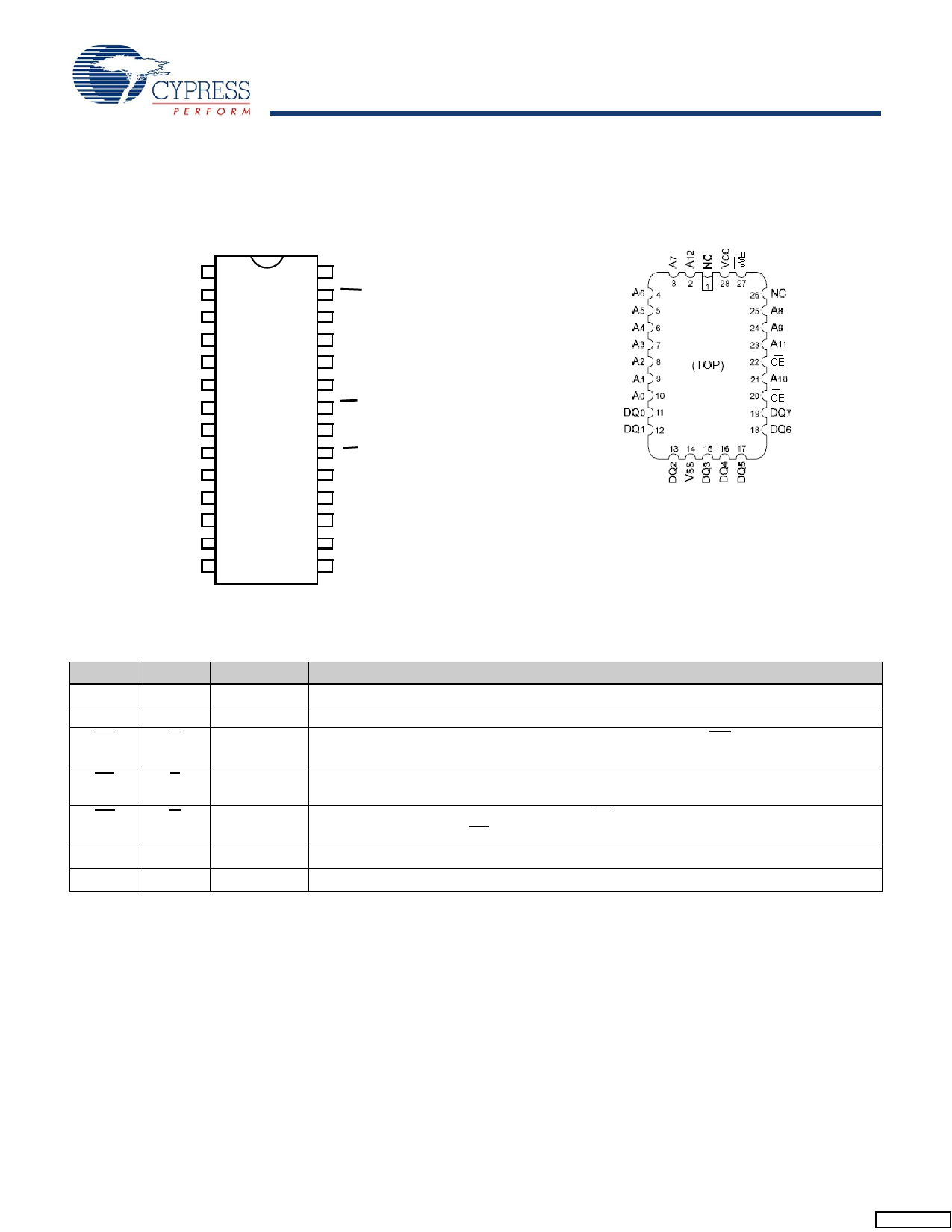
Figure 1. Pin Diagram - 28-Pin DIP
1&
$
$
$
$
$
$
$
$
$
'4
'4
'4
966
723
9&&
:(
1&
$
$
$
2(
$
&(
'4
'4
'4
'4
'4
STK11C68-5 (SMD5962-92324)
Figure 2. Pin Diagram - 28-Pin LLC
Pin Definitions
Pin Name Alt
A0–A12
DQ0-DQ7
WE
W
CE
E
OE
G
VSS
VCC
I/O Type
Description
Input
Address Inputs. Used to select one of the 8,192 bytes of the nvSRAM.
Input/Output Bidirectional Data I/O Lines. Used as input or output lines depending on operation.
Input
Write Enable Input, Active LOW. When the chip is enabled and WE is LOW, data on the I/O
pins is written to the specific address location.
Input
Chip Enable Input, Active LOW. When LOW, selects the chip. When HIGH, deselects the
chip.
Input
Output Enable, Active LOW. The active LOW OE input enables the data output buffers during
read cycles. Deasserting OE HIGH causes the I/O pins to tristate.
Ground Ground for the Device. The device is connected to ground of the system.
Power Supply Power Supply Inputs to the Device.
Document Number: 001-51001 Rev. *A
Page 2 of 15
[+] Feedback
Share Link: 