SST31LF041 데이터 시트보기 (PDF) - Silicon Storage Technology
부품명
상세내역
일치하는 목록
SST31LF041 Datasheet PDF : 26 Pages
| |||
4 Mbit Flash + 1 Mbit or 256 Kbit SRAM ComboMemory
SST31LF041 / SST31LF041A / SST31LF043 / SST31LF043A
Data Sheet
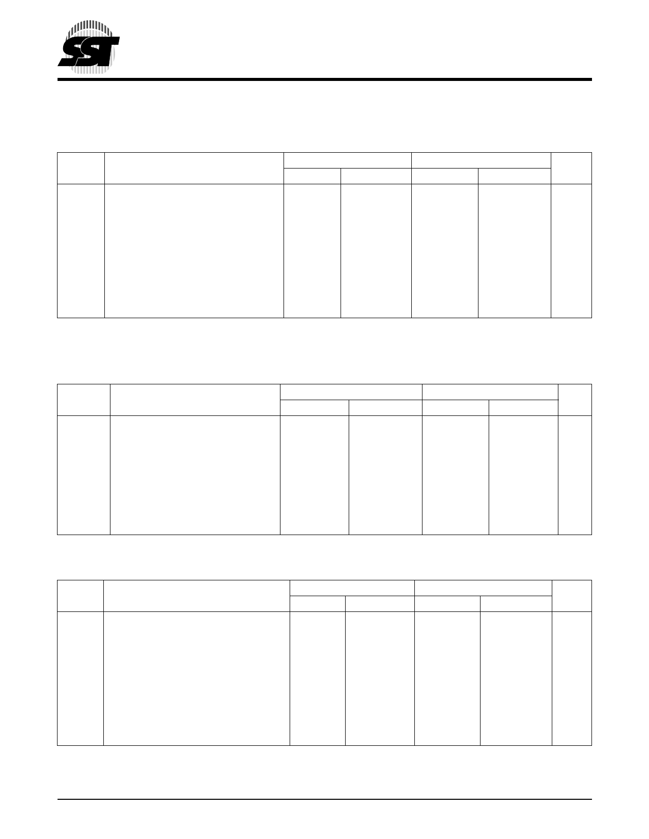
AC CHARACTERISTICS
TABLE 9: SRAM MEMORY BANK CYCLE TIMING PARAMETERS (VDD = 3.0-3.6V)
SST31LF041/043-70
SST31LF041A/043A-300
Symbol Parameter
Min
Max
Min
Max
Units
TRCS
Read Cycle Time
70
300
TBES
Bank Enable Access Time
70
300
TAAS
Address Access Time
70
300
TOES1
Output Enable Access Time
35
150
TBLZS2 BES# to Active Output
0
0
TOLZS1 Output Enable to Active Output
0
0
TBHZS1 BES# to High-Z Output
25
30
TOHZS1 Output Disable to High-Z Output
25
30
TOHS
Output Hold from Address Change
0
10
1. No TOES value for SST31LF041A/043A
2. This parameter is measured only for initial qualification and after a design or process change that could affect this parameter.
ns
ns
ns
ns
ns
ns
ns
ns
ns
T9.8 349
TABLE 10: SRAM MEMORY BANK WRITE CYCLE TIMING PARAMETERS (VDD = 3.0-3.6V)
SST31LF041/043-70
SST31LF041A/043A-300
Symbol Parameter
Min
Max
Min
Max
TWCS
Write Cycle Time
70
300
TBWS
Bank Enable to End-of-Write
60
230
TAWS
Address Valid to End-of-Write
60
230
TASTS
Address Set-up Time
0
0
TWPS
Write Pulse Width
60
200
TWRS
Write Recovery Time
0
0
TDSS
Data Set-up Time
30
150
TDHS
Data Hold from Write Time
0
0
Unit
ns
ns
ns
ns
ns
ns
ns
ns
T10.5 349
TABLE 11: FLASH READ CYCLE TIMING PARAMETERS (VDD = 3.0-3.6V)
SST31LF041/043-70
SST31LF041A/043A-300
Symbol Parameter
Min
Max
Min
Max
Units
TRC
TBE
TAA
TOE
TBLZ1
TOLZ1
TBHZ1
TOHZ1
TOH1
Read Cycle Time
Bank Enable Access Time
Address Access Time
Output Enable Access Time
BEF# Low to Active Output
OE# Low to Active Output
BEF# High to High-Z Output
OE# High to High-Z Output
Output Hold from Address Change
70
300
70
300
70
300
40
150
0
0
0
0
15
60
15
60
0
0
1. This parameter is measured only for initial qualification and after a design or process change that could affect this parameter.
ns
ns
ns
ns
ns
ns
ns
ns
ns
T11.5 349
©2001 Silicon Storage Technology, Inc.
10
S71107-03-000 5/01 349
Share Link: 