54HC4011 데이터 시트보기 (PDF) - STMicroelectronics
부품명
상세내역
일치하는 목록
54HC4011 Datasheet PDF : 13 Pages
| |||
M54/M74HC4511
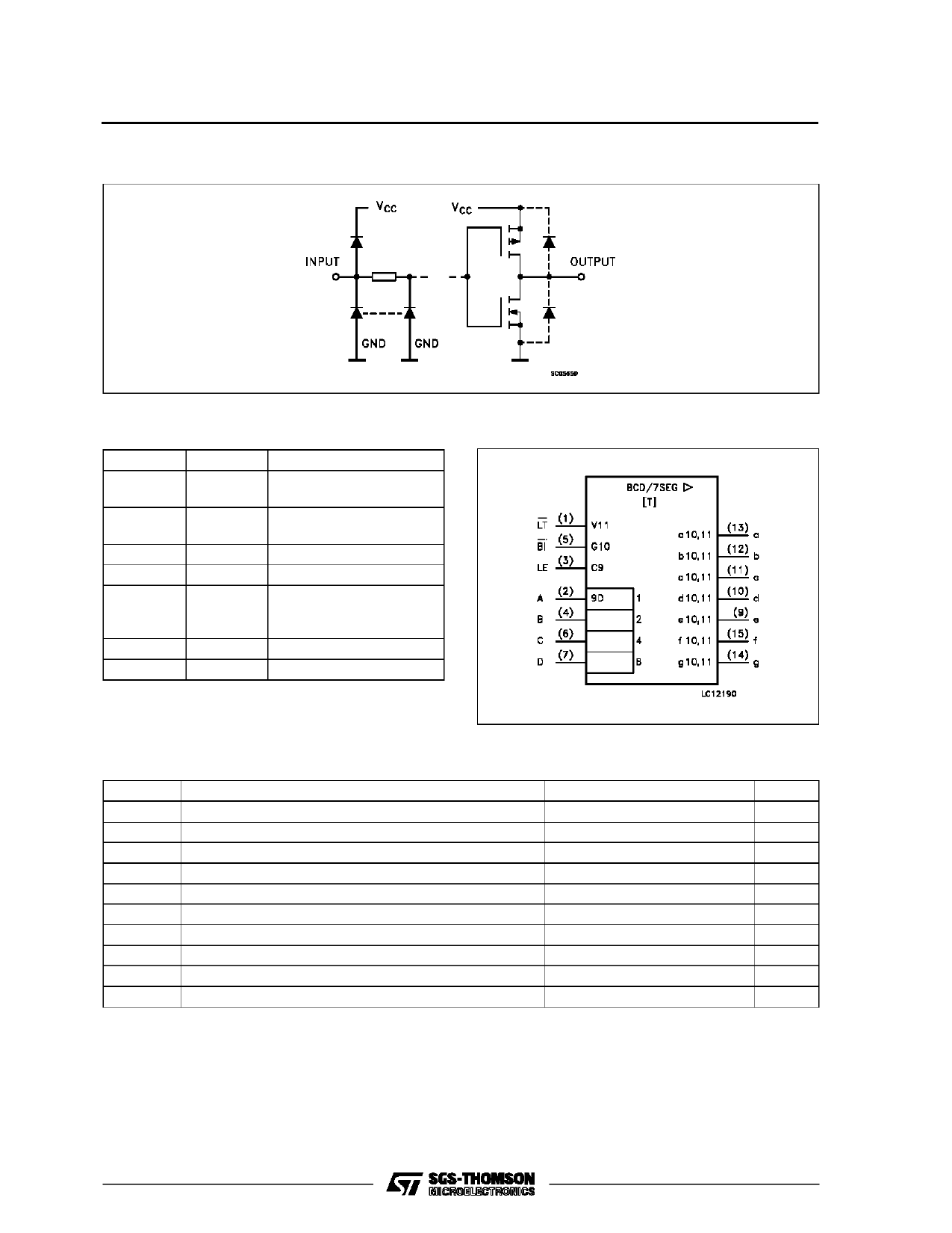
INPUT AND OUTPUT EQUIVALENT CIRCUIT
PIN DESCRIPTION
PIN No
3
4
5
7, 1, 2, 6
13, 12, 11,
10, 9 , 15,
14
8
16
SYMBOL
LT
BI
LE
A to D
a to g
GND
VCC
NAME AND FUNCTION
Lamp Test Input (Active
LOW)
Ripple Blanking Input
(Active LOW)
Latch Enable Input
BCD Address Inputs
Segment Outputs
Ground (0V)
Positive Supply Voltage
IEC LOGIC SYMBOL
ABSOLUTE MAXIMUM RATINGS
Symbol
Parameter
Value
Unit
VCC
Supply Voltage
-0.5 to +7
V
VI
DC Input Voltage
-0.5 to VCC + 0.5
V
VO
DC Output Voltage
-0.5 to VCC + 0.5
V
IIK
DC Input Diode Current
± 20
mA
IOK
DC Output Diode Current
± 20
mA
IO
DC Output Source Sink Current Per Output Pin
-35/25
mA
ICC or IGND DC VCC or Ground Current
+150/-50
mA
PD
Power Dissipation
500 (*)
mW
Tstg
Storage Temperature
TL
Lead Temperature (10 sec)
-65 to +150
oC
300
oC
Absolute Maximum Ratings are those values beyond which damage to the device may occur. Functional operation under these condition isnotimplied.
(*) 500 mW: ≅ 65 oC derate to 300 mW by 10mW/oC: 65 oC to 85 oC
4/13
Share Link: 