SPX29301 데이터 시트보기 (PDF) - Signal Processing Technologies
부품명
상세내역
일치하는 목록
SPX29301 Datasheet PDF : 11 Pages
| |||
ELECTRICAL CHARACTERISTICS
at VIN=VOUT + 1V and IOUT = 10mA, CIN = 6.8μF, COUT = 10μF, TA = 25°C, unless otherwise specified. The Boldface applies
over the junction temperature range. Adjustable versions are set to 5.0V.
PARAMETER
CONDITIONS
FLAG OUTPUT (ERROR COMPARATOR)
TYP
MIN MAX UNITS
SPX29301/03
Output Leakage
VOH=16V
0.01
Current
Output Low Voltage
Device set for 5V,VIN=4.5V, IOL=250μA
220
1
μA
2
300
mV
400
Upper Threshold
Voltage
Device set for 5V, (Note 9)
60
40
mV
25
Lower Threshold
Voltage
Device set for 5V, (Note 9)
75
95
mV
140
Hysteresis
ENABLE Input
Device set for 5V, (Note 9)
15
mV
SPX29301/02
Input Logic Voltage
Low (OFF)
High (ON)
ENABLE Input Pin
Regulator Output
Current in Shutdown
Thermal Resistance
VIN<10V
VEN=16V
VEN=0.8V
(Note 10)
TO-200 Junction to Case, at Tab
TO-220 Junction to Ambient
TO-263 Junction to Case, at Tab
TO-263 Junction to Ambient
0.8
V
2.4
100
600
μA
750
1
μA
2
10
500
μA
3
°C/W
60
3
60
NOTES:
Note 1: Maximum positive supply voltage of 20V must be of limited duration (<100ms) and duty cycle of less than 1%. The maximum continuous supply
voltage is 16V.
Note 2: Full load current (IFL) is defined as 3.0A.
Note 3: Dropout voltage is defined as the input to output differential when the output voltage drops to 99% of its nominal value.
Note 4: VIN = VOUT (NOMINAL) +1V. For example, use VIN = 4.3V for a 3.3V regulator. Employ pulse-testing procedures to minimize temperature rise.
Note 5: Ground pin current is the regulator quiescent current. The total current drawn from the source is the sum of the load current to the ground current.
Note 6: Output voltage temperature coefficient is defined as the worst case voltage change divided by the total temperature range
Note 7: Thermal regulation is defined as the change in output voltage at time T after a change in power dissipation is applied, excluding load / line regulation effects.
Specifications for a 200mA load pulse as VIN = 20V (a 4W pulse) for t = 10ms.
Note 8: VREF≤ VOUT ≤ (VIN-1), 2.3V≤VIN ≤ 16V, 10mA ≤ IL ≤ IFL, Tj < Tjmax.
Note 9: Comparator threshold is expressed in terms of a voltage differential at the Adjust terminal below the nominal reference voltage measured 6V input. To
express these thresholds in terms of output voltage change, multiply the error amplifier gain = VOUT/VREF = (R1 + R2)/R2. For example, at a programmable
output voltage of 5V, the Error output is guaranteed to go low when the output drops by 95mVx 5V/ 1.240V = 38mV. Threshold remain constant as a percent of
VOUT as VOUT is varied, with the dropout warning occurring at typically 5% below nominal, 7.7% guaranteed.
Note 10: VEN ≤ 0.8V and VIN ≤ 16V, VOUT = 0.
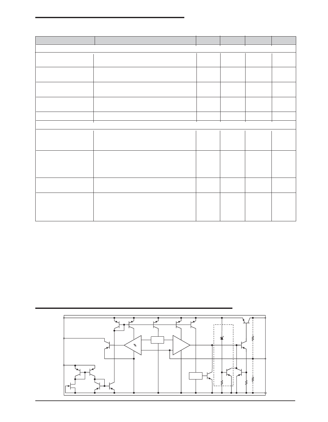
BLOCK DIAGRAM
IN
OUT
FLAG
+ 1.180V Reference 1.240V +
O.V
I LIMIT
28V
R1*
-
-
ADJ
EN
Thermal
Shutdown
R2*
Date: 9/5/06 Rev C
SPX29300/01/02/03 3A Low Dropout Voltage Regulator
3
GND
© 2006 Sipex Corporation
Share Link: 