SPX2931(2004) 데이터 시트보기 (PDF) - Signal Processing Technologies
부품명
상세내역
일치하는 목록
SPX2931 Datasheet PDF : 8 Pages
| |||
ABSOLUTE MAXIMUM RATINGS
Power Dissipation (note 3) ........................................ Internally limited
Lead Temp (soldering, 5 seconds) ............................................ 260°C
Storage Temperature Range ..................................... -65°C to +150°C
Input Supply Voltage Range ............................................. -0.3 to +30V
ESD Rating (note 4) ...................................................................... 2kV
RECOMMENDED OPERATING CONSITIONS
Input Voltage Range ........................................................... 3.0 to 26V
Operating Junction Temperature Range ..................... -40°C to 125°C
TO-92ΘJA ............................................................................... 160°C/W
SOT-89ΘJA ............................................................................ 110°C/W
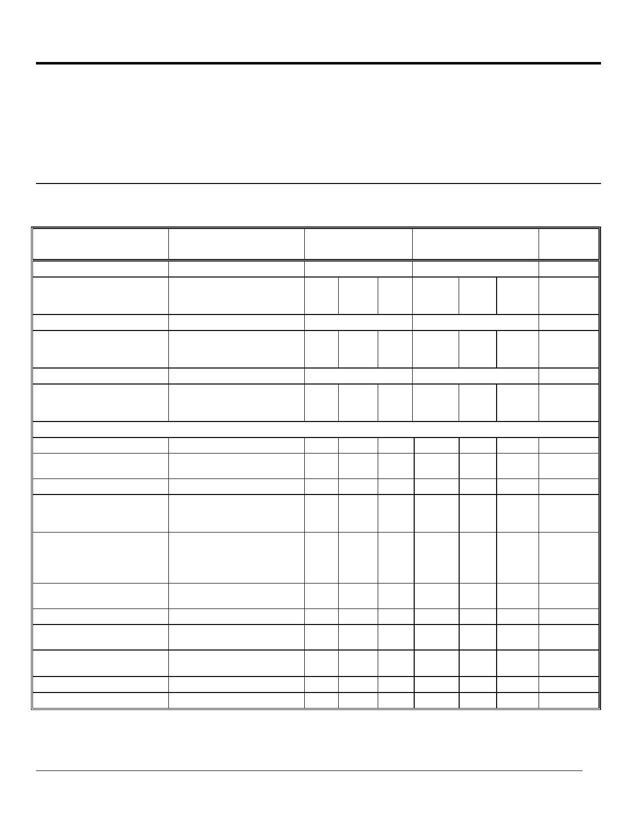
ELECTRICAL CHARACTERISTICS
at VIN=6V, TA = 25°C, IO = 10 mA, COUT = 100 µF, unless otherwise specified. (Note 1)
PARAMETER
CONDITIONS
MIN TYP MAX
MIN TYP MAX
3.3V Version
Output Voltage (Note 2) 4V < VIN <26V,
IO = 100 mA over temp.
3.234 3.300 3.366
3.201 3.300 3.399
3.201 3.300 3.399
3.135 3.300 3.465
3.5V Version
Output Voltage (Note 2) 4.5V < VIN < 26V,
IO = 100mA Over Temp.
3.430 3.500 3.570
3.395 3.500 3.605
3.395 3.500 3.605
3.325 3.500 3.675
All Voltage Options
Long Term Stability
20
20
Line Regulation
9V<VIN<16V,
4.5V<VIN<26V
2.0 10
4.0 30
Load Regulation
5mA<IO< 150mA
14
50
Dropout Voltage
IO =10mA
IO =150mA
0.05 0.2
0.3 0.6
Quiescent Current
IO =10mA, 4.5V<VIN<26V
-40°C<Tj<85°C
IO =150mA, VIN=14V,
TJ =25°C
0.4 1.0
15
Output Noise Voltage 10Hz-100kHz, COUT =100µF
500
Ripple Rejection
FO =120Hz
80
Maximum Operational
Input Voltage
26
4.0 30
14 50
0.05 0.2
0.3 0.6
0.4 1.0
15
500
80
26
Maximum Line Transient RL = 500Ω, 100ms
Reverse Polarity Input VO> -0.3V, RL= 500Ω
Voltage, DC
60
70
-15 -30
50
70
-15 -30
Reverse Polarity Input 1% Duty Cycle, τ <100ms
Voltage, Transient
RL=500Ω
-50 -80
-50 -80
NOTES:
Note 1: See TYPICAL APLICATIONS notes to ensure constant junction temperature, low duty cycle pulse testing used.
Note 2: All limits are at 25°C or over the full operationg junction temperature range of -40°C to +125°C.
Note 3: The maximum power dissipation is a function of maximum junction temperature, total thermal resistance, and ambient temperature.
Note 4: Human body model, 100pF discharged through 1.5kΩ.
UNITS
V
V
mV/1000hr
mV
mV
V
mA
µVRMS
dB
V
V
V
V
Date: 05/25/04
SPX2931 100mA Low Dropout Voltage Regulator
2
© Copyright 2004 Sipex Corporation
Share Link: 