SP6680EU/TR 데이터 시트보기 (PDF) - Signal Processing Technologies
부품명
상세내역
일치하는 목록
SP6680EU/TR Datasheet PDF : 12 Pages
| |||
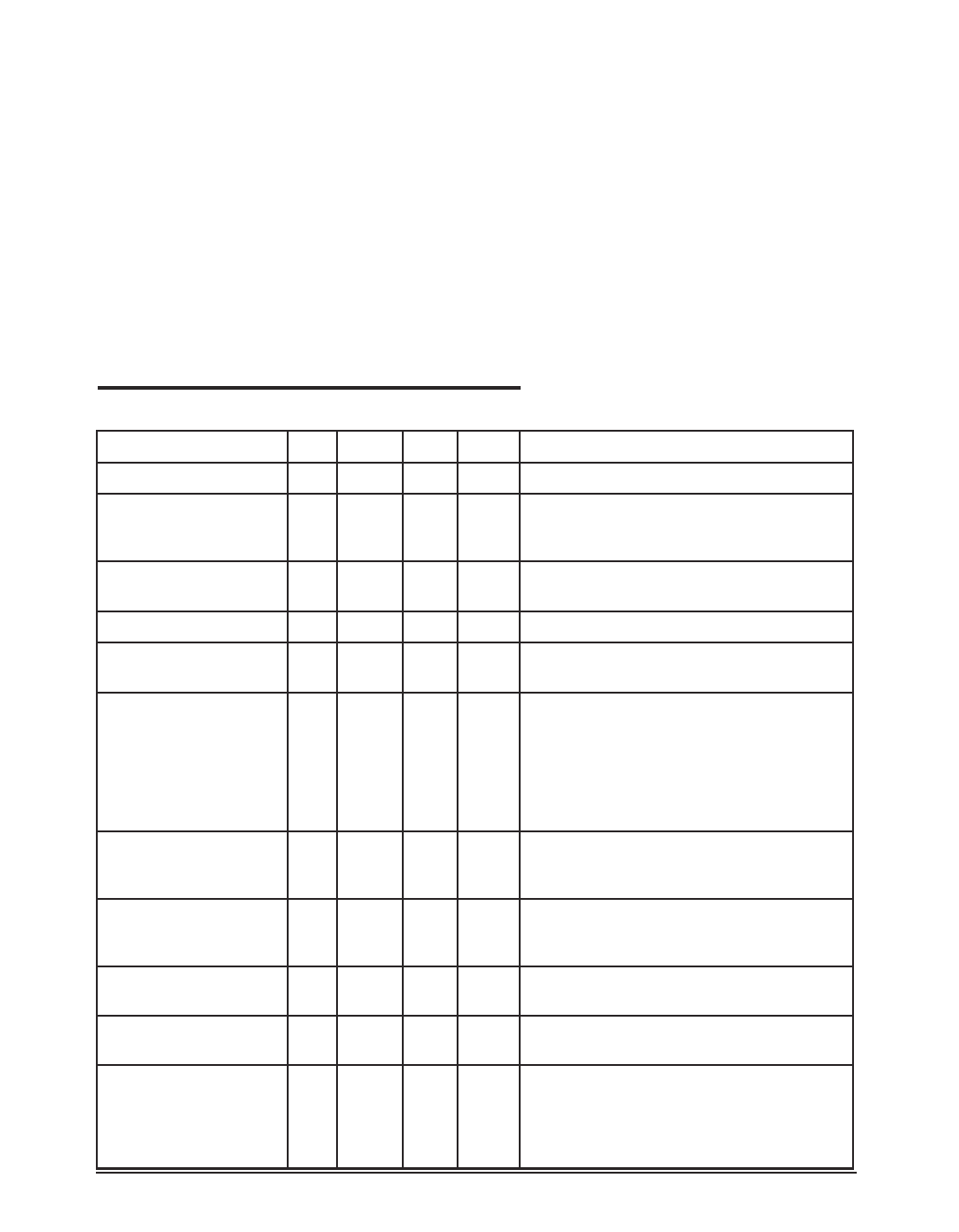
ABSOLUTE MAXIMUM RATINGS
These are stress ratings only and functional operation
of the device at these ratings or any other above those
indicated in the operation sections of the specifications
below is not implied. Exposure to absolute maximum
rating conditions for extended periods of time may
affect reliability.
VIN.........................................................-0.3V to +7.0V
VOUT......................................................-0.3V to +7.0V
IOUT....................................................................100mA
Storage Temperature........................-65˚C to +150˚C
Power Dissipation Per Package
10-pin mSOIC
(derate 8.84mW/OC above +70OC)..................720mW
Junction Temperature........................................125˚C
ELECTRICAL CHARA CTERISTICS
VIN = +2.7 to +6.3V, fCLK = 32.768kHz, CIN = 4.7µF (ceramic), CF1 = CF2 = COUT = 2.2µF, (ESR = 0.03 Ω) and TAMB = -40°C to +85°C unless otherwise
noted.
PARAMETER
MIN. TYP. MAX. UNITS
CONDITIONS
Supply Voltage, VIN
Quiescent Current, I
Q
In-Rush Current into VIN,
IINRUSH
Off Current, IOFF
Input Clock Frequency,
fCLK
Pump Frequency, fPUMP
(Note 2)
2.75 3.6
6.3
75
150
170 300
800 1500
500
4.4
10
32.768
V
f = f /4
PUMP CLK
µA
fCLK = fPUMP
fPUMP = fCLK x 8
VIN = 4.2V
mA 2.7V<VIN<6.3V, Note 1
µA VIN = 4.2V, clock not present, -40˚ C to +70˚ C
kHz Operational (supplied externally)
0
32.768
8.192
262.14
16.7
fCLK
C/4pin input Cx8pin input
no input
X
X
kHz
present
low
low
present
high
low
present
X
high
high
low
low
Input Threshold Voltage
VIL
VIH
Input Current
IIN(low)
IIN(high)
Mode Transition Voltage,
X1.5 to X2, VIN falling
Hysteresis for Mode
Transition Voltage
1.3
3.55
3.55
0.1
1.0
3.70
3.70
50
0.4
V
Digital inputs = fCLK, fCLK/4, fCLK x 8
Digital inputs = fCLK, fCLK/4, fCLK x 8
10
10
3.85
3.85
µA Digital inputs = fCLK, fCLK/4, fCLK x 8
Digital inputs = fCLK, fCLK/4, fCLK x 8
V
fpump = fCLK/4, ILOAD = 1mA
fpump, fCLK, ILOAD = 5mA
mVpp VIN rising to VIN falling
Transient Response:
Maximum Transient
Amplitude
ILOAD
∆t
fPUMP
1.5
% 100µA to 2mA
5µs
8.192kHz
1.5
2mA to 20mA
5µs
32.768kHz
1.5
20mA to 60mA
5µs
262.14kHz
Date: 5/25/04
SP6680 High Efficiency Buck/Boost Charge Pump Regulator
2
© Copyright 2004 Sipex Corporation
Share Link: 