U62H64SK35L 데이터 시트보기 (PDF) - Zentrum Mikroelektronik Dresden AG
부품명
상세내역
일치하는 목록
U62H64SK35L Datasheet PDF : 9 Pages
| |||
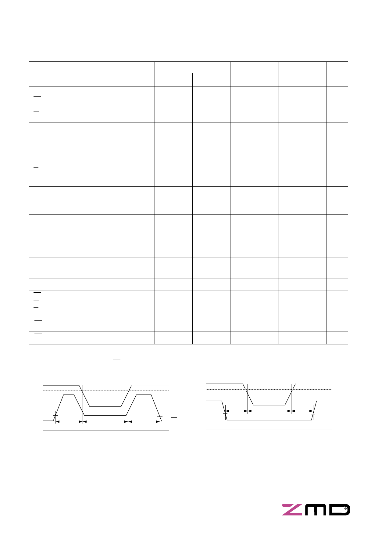
U62H64
Switching Characteristics
Time to Output in Low-Z from
E1 LOW or E2 HIGH
G LOW
W HIGH
Cycle Time
Write Cycle Time
Read Cycle Time
Access Time
E1 LOW or E2 HIGH to Data Valid
G LOW to Data Valid
Address to Data Valid
Pulse Widths
Write Pulse Width
Chip Enable to End of Write
Setup Times
Address Setup Time
Chip Enable to End of Write
Write Pulse Width
Data Setup Time
Data Hold Time
Address Hold from End of Write
Output Hold Time from Address Change
E1 HIGH or E2 LOW to Output in High-Z
W LOW to Output in High-Z
G HIGH to Output in High-Z
E1 LOW or E2 HIGH to Power-Up
E1 HIGH or E2 LOW to Power-Down
Symbol
Alt.
IEC
tLZCE
tLZOE
tLZWE
tWC
tRC
tACE
tOE
tAA
tWP
tCW
tAS
tCW
tWP
tDS
tDH
tAH
tOH
tHZCE
tHZWE
tHZOE
tPU
tPD
ten(E)
ten(G)
ten(W)
tcW
tcR
ta(E)
ta(G)
ta(A)
tw(W)
tw(E)
tsu(A)
tsu(E)
tsu(W)
tsu(D)
th(D)
th(A)
tv(A)
tdis(E)
tdis(W)
tdis(G)
Min.
5
0
0
35
35
20
25
0
25
20
15
0
0
5
0
Unit
Max.
ns
ns
ns
ns
ns
35
ns
15
ns
35
ns
ns
ns
ns
ns
ns
ns
ns
ns
ns
15
ns
15
ns
12
ns
ns
35
ns
Data Retention Mode E1-Controlled
Data Retention Mode E2-Controlled
4.5 V
2.2 V
tDR
0V
VCC(DR) ≥ 2 V
Data Retention
VCC
2.2 V
trec
E1
VE2(DR) ≥ VCC(DR) - 0.2 V or VE2(DR) ≤ 0.2 V
VCC(DR) - 0.2 V ≤ VE1(DR) ≤ VCC(DR) + 0.3 V
4.5 V
tDR
0.8 V
VCC(DR) ≥ 2 V
Data Retention trec
VCC
E2
0.8 V
0V
VE1(DR) ≥ VCC(DR) - 0.2 V or VE1(DR) ≤ 0.2 V
VE2(DR) ≤ 0.2 V
April 20, 2004
Chip Deselect to Data Retention Time tDR:
Operating Recovery Time at VCC(DR)
trec:
min 0 ns
min tcR
5
Share Link: 