AK4363VF 데이터 시트보기 (PDF) - Asahi Kasei Microdevices
부품명
상세내역
일치하는 목록
AK4363VF Datasheet PDF : 29 Pages
| |||
ASAHI KASEI
[AK4363]
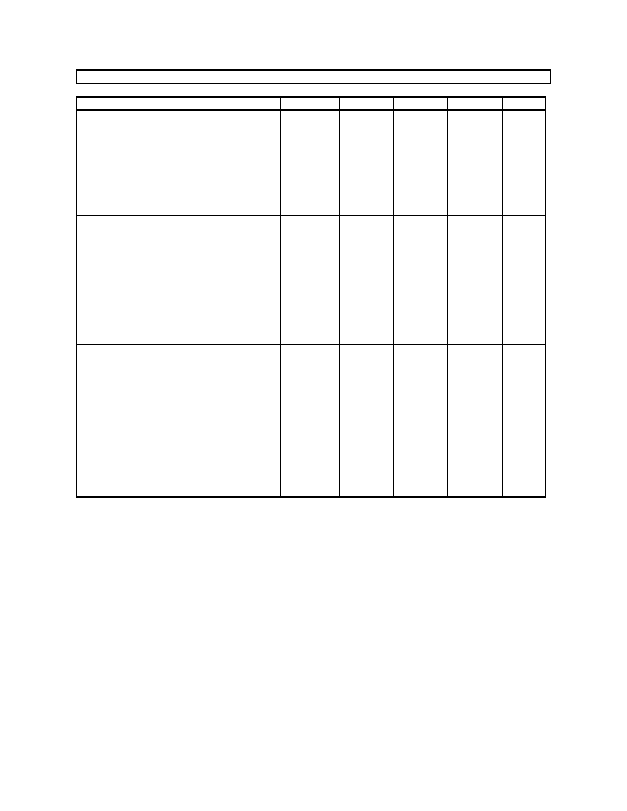
SWITCHING CHARACTERISTICS
(Ta=25°C; AVDD, DVDD=2.7∼5.5V; CL=20pF)
Parameter
Symbol
min
typ
27MHz Input (PLL mode):
Frequency
f27M
27
Pulse Width Low
t27ML
14
Pulse Width High
t27MH
14
Master Clock Input (External mode):
Frequency
128fs/256fs/512fs/1024fs
fCLK
4.096
192fs/384fs/768fs/1536fs
fCLK
6.144
Duty Cycle
dCLK
40
MCKO Output (PLL mode):
Frequency
fMCKO
4.096
Duty Cycle
dMCKO
40
Rise time (20% to 80% DVDD)
trMCKO
2
Fall time (80% to 20% DVDD)
tfMCKO
2
LRCK:
(Note 9)
Frequency
Half Speed Mode (DFS1-0 = “11”)
fsh
16
Normal Speed Mode (DFS1-0 = “00”) fsn
32
Double Speed Mode (DFS1-0 = “01”)
fsd
64
Duty Cycle
Duty
45
Serial Interface Timing:
BICK Period
Half Speed Mode
tBCK
1/128fs
Normal Speed Mode
tBCK
1/128fs
Double Speed Mode
tBCK
1/64fs
BICK Pulse Width Low
tBCKL
70
BICK Pulse Width High
tBCKH
70
BICK “↑” to LRCK Edge
(Note 10)
tBLR
40
LRCK Edge to BICK “↑”
(Note 10)
tLRB
40
SDTI Hold Time
tSDH
40
SDTI Setup Time
tSDS
40
Power-down & Reset Timing
PDN Pulse Width
(Note 11)
tPDW
150
max
24.576
36.864
60
36.864
60
24
48
96
55
Note: 9. If sampling speed mode (DFS0-1) changes, please reset by PDN pin or RSTN bit.
10. BICK rising edge must not occur at the same time as LRCK edge.
11. The AK4363 can be reset by PDN pin “L” upon power up.
If CKS0-2 or DFS0-1 changes, the AK4363 should be reset by PDN pin or RSTN bit.
Units
MHz
ns
ns
MHz
MHz
%
MHz
%
ns
ns
kHz
kHz
kHz
%
ns
ns
ns
ns
ns
ns
ns
ns
ns
ns
MS0015-E-01
- 10 -
2000/07
Share Link: 