SC16313 데이터 시트보기 (PDF) - Silan Microelectronics
부품명
상세내역
일치하는 목록
SC16313 Datasheet PDF : 9 Pages
| |||
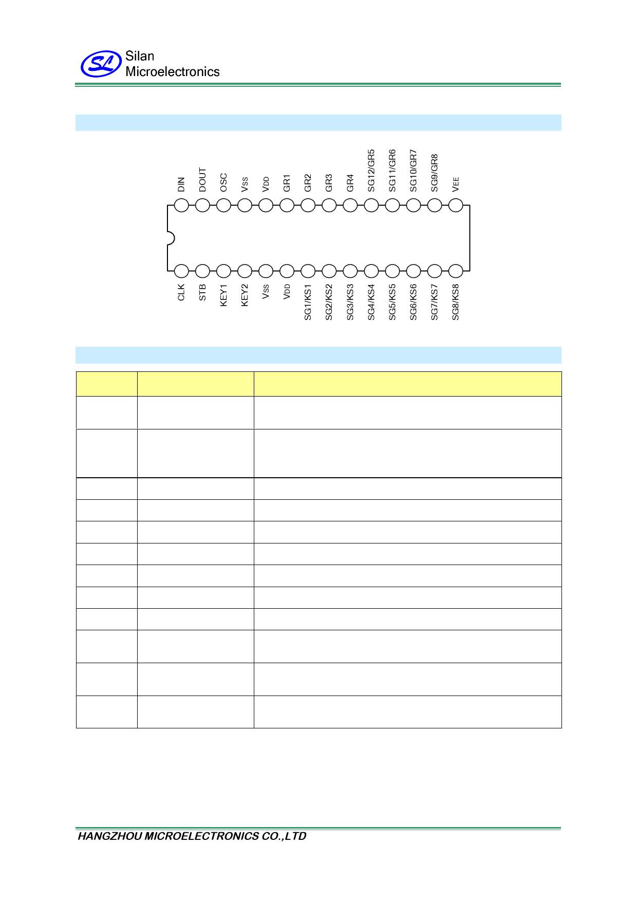
PIN CONFIGURATION
SC16313
28 27 26 25 24 23 22 21 20 19 18 17 16 15
SC16313
1 2 3 4 5 6 7 8 9 10 11 12 13 14
PIN DESCRIPTION
Pin NO.
1
2
3, 4
5, 25
6, 24
7 to 14
15
16 to 19
20 to 23
26
27
28
Symbol
CLK
STB
KEY1 to KEY2
VSS
VDD
SG1/KS1 to SG8/KS8
VEE
SG9/GR8 ~SG12/GR5
GR4 to GR1
OSC
DOUT
DIN
Description
Reads serial data at the rising edge and outputs data at the falling
edge.
After the STB has fallen, The data input can be processed; the first
data is regard as a command. When this pin is “HIGH”, CLK is
ignored.
The data input to these pins is latched at the end of display cycle.
Logic ground pin
Logic power supply
Segment output pins. It also functions as key source.
VDD – 35 V max
These pins are selectable for segment or grid output
Grid output pins
This pin connects a resistor to VDD to determine the oscillation
frequency.
Outputs serial data at the falling edge of the shift clock (starting from
the lower bit).
Inputs serial data at the rising edge of the shift clock (starting from
the lower bit).
HANGZHOU MICROELECTRONICS CO.,LTD
Http: www.silan.com.cn
REV:1.2 2003.08.28
Page 3 of 10
Share Link: 