SC1628 데이터 시트보기 (PDF) - Semtech Corporation
부품명
상세내역
일치하는 목록
SC1628 Datasheet PDF : 4 Pages
| |||
January 30, 1998
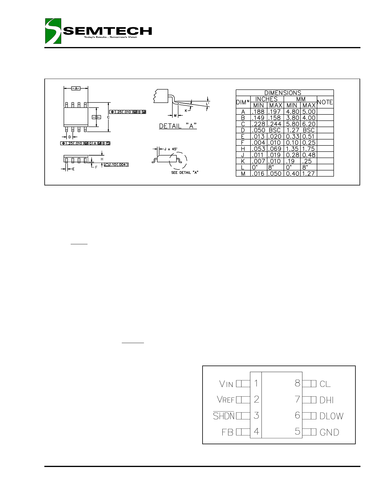
DEVICE OUTLINE - SO-8
HIGH-EFFICIENCY STEP-UP
DC-DC CONVERTER
SC1628
PIN DESCRIPTIONS
PIN 1: VIN 4V to 24V input supply voltage.
PIN 2: VREF
1.22V reference output. Bypass with
a 0.047µF capacitor to GND.
Sourcing capability is guaranteed to
be greater than 250µA.
PIN 3:
SHDN Logical input to shutdown the chip:
>1.5V = normal operation,
GND = shutdown.
Cannot be floating or forced greater
than 15V. In shutdown mode DLOW
and DHI pins are low.
PIN 4: FB
Feedback signal input to comparator.
Connecting a resistance R1 to VOUT
and a resistance R2 to GND yields
the output voltage:
VOUT
=
R1+ R2
R2
×
VREF
(refer to typical application circuit).
PIN 5: GND Power ground.
PIN 6:
DLOW
Driver sinking output. Connected to
the gate of the external N-channel
MOSFET or the base of the NPN
bipolar transistor.
PIN 7: DHI
PIN 8: CL
Driver sourcing output. Connected to
DLOW when using an external N-
channel MOSFET. When using an
external NPN bipolar transistor,
connect a base resistance RB from
this pin to DLOW. RB value depends
upon VIN, the inductor value and the
NPN current gain.
Current-limit input. The threshold
voltage is 60mV from VIN. This pin
clamps the switch peak current under
abnormal conditions.
PIN CONFIGURATION
© 1997 SEMTECH CORP.
652 MITCHELL ROAD NEWBURY PARK CA 91320
Share Link: 