RT9278 데이터 시트보기 (PDF) - Richtek Technology
부품명
상세내역
일치하는 목록
RT9278 Datasheet PDF : 13 Pages
| |||
Preliminary
RT9278
Functional Pin Description
Pin No.
Pin Name
Pin Function
1
FB
Feedback Input Pin.
2
COMP
Feedback Compensation Pin.
3
GND
Ground.
4
EN
Enable Input Pin
5
LX
Switch Node.
6
VOUT
Output Pin
7
VDD
Device Input Power Pin.
8
PGND
Power Ground.
9
LDRI
Linear Controller Driver Output.
10
LFB
Linear Controller Feedback Input.
Exposed Pad (11) GND
The exposed pad must be soldered to a large PCB and connected to
GND for maximum power dissipation.
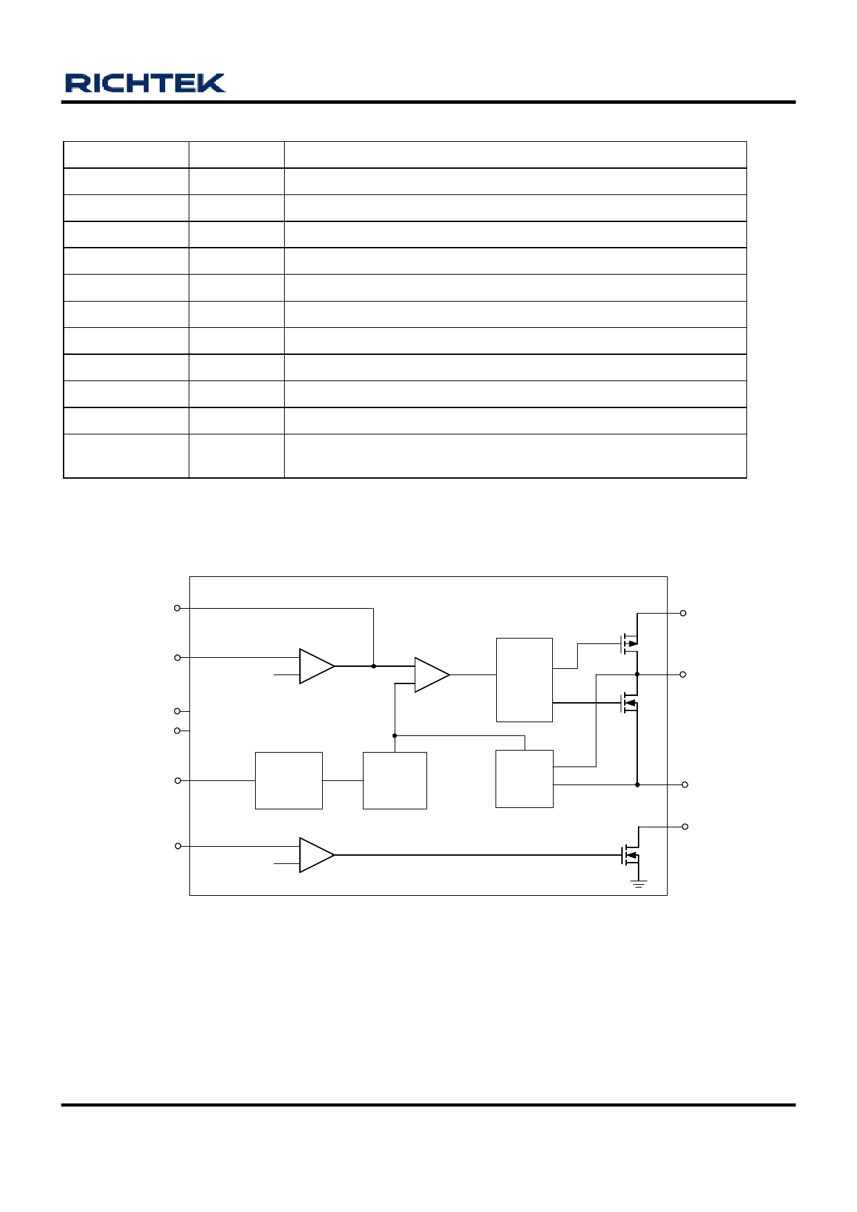
Function Block Diagram
COMP
FB
VDD
GND
EN
VREF = 0.8V
Error
AMPLIFIER
-
+
Error
Comparator
-
+
Oscillator
and
Shutdown
Control
Slope
Compen-
sation
LFB
-
VREF = 0.2V
+
Control
and
Driver
Logic
Current
Sense
VOUT
LX
PGND
LDRI
DS9278-04 August 2007
www.richtek.com
5
Share Link: 