RT9275 데이터 시트보기 (PDF) - Richtek Technology
부품명
상세내역
일치하는 목록
RT9275 Datasheet PDF : 14 Pages
| |||
RT9275
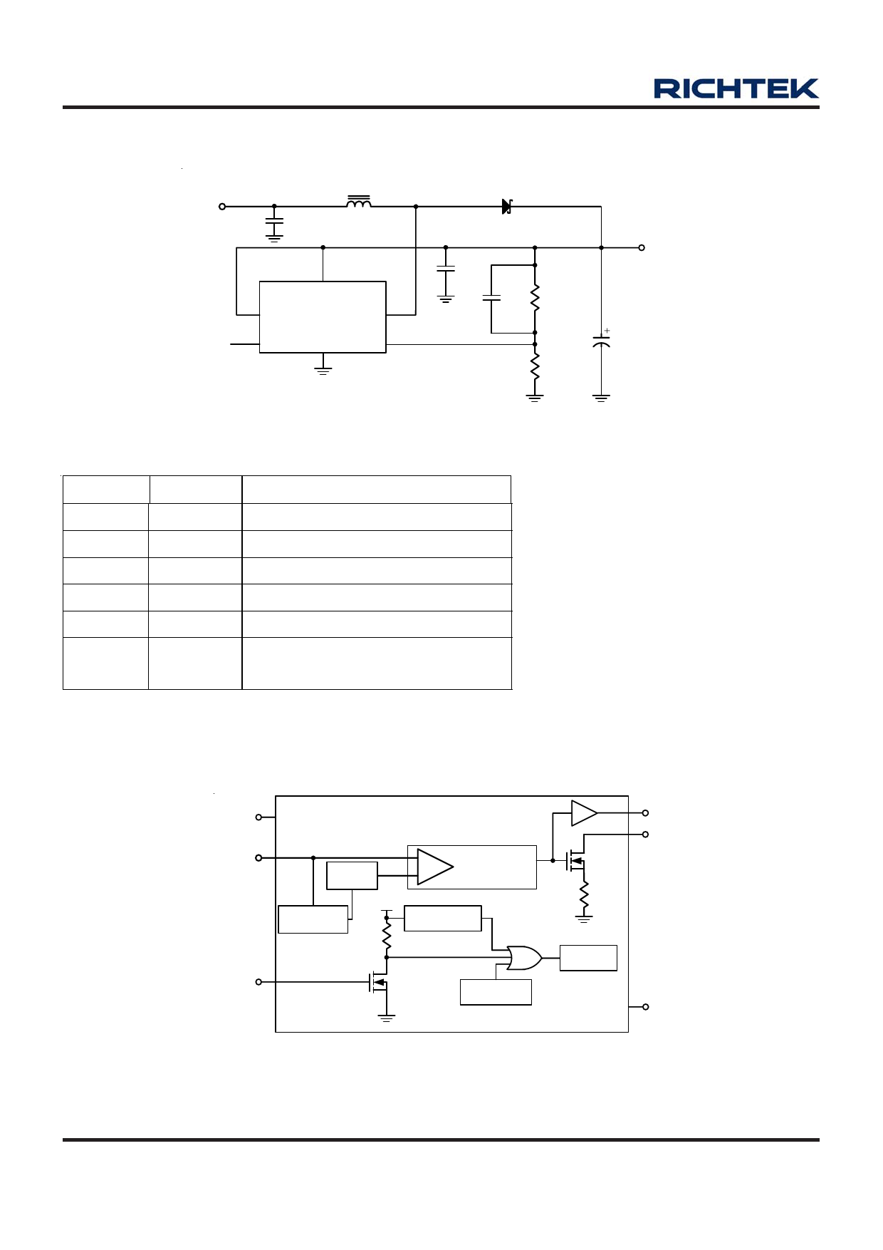
Typical Application Circuit
Preliminary
L1
4.7 uH
VIN
C3
10uF
VDD
EN RT9275 LX
EXT GND FB
D1
FS1J2E
C2
1uF
C4
R1
6.8pF/ 2M/3M
3.3pF
R2
980k/1M
VOUT
3.3V/5V
C1
10uF/20uF
Functional Pin Description
Pin No.
1
2
3
4
5
6
Pin Name
EN
EXT
GND
LX
VDD
FB
Pin Function
Chip Enable (Active High)
Output pin for driving external NMOS
Ground
Pin for switching
Input positive power pin of RT9275
Feedback input pin. Internal reference
voltage for the error amplifier is 1.25V.
Function Block Diagram
VDD
FB
-
Loop Control
Bandgap/
+
Circuit
Soft Start VREF
Under Voltage
Protection
VDD
Over Voltage
Protection
EN
Over Temp.
Detector
Function
Suspend
EXT
LX
GND
www.richtek.com
2
DS9275-06 March 2007
Share Link: 