RT9272 데이터 시트보기 (PDF) - Richtek Technology
부품명
상세내역
일치하는 목록
RT9272 Datasheet PDF : 11 Pages
| |||
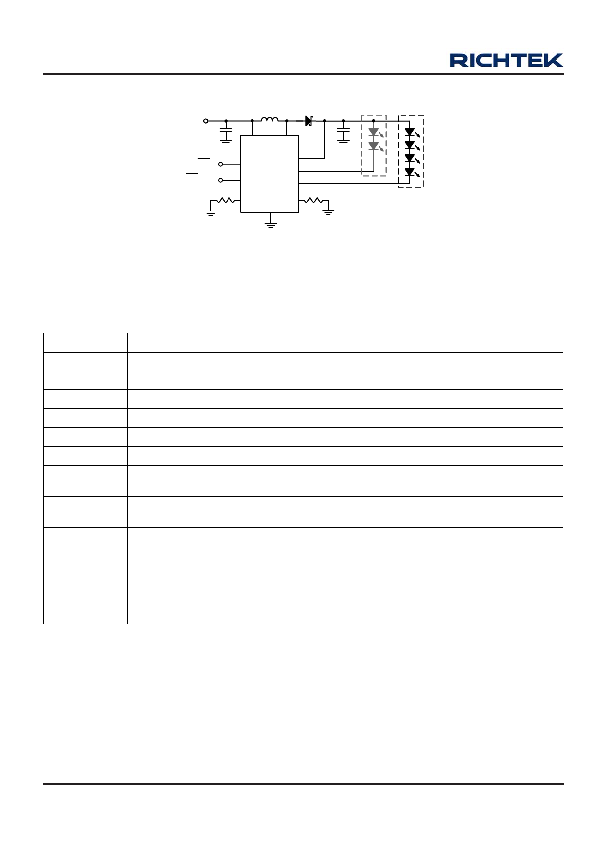
RT9272
Preliminary
CIN
2.2uF
L
SS0520
4.7uF DSH
VIN
4
10
VCC LX
Chip Enable
7
9
EN
SP
RT9272
OVP
CH1
CH2
8
5
3
R1 6 FB1
FB2 2 R2
GND
1
COUT
1uF
Sub-Panel
Main Panel
Figure 1. 2LEDs for Sub panel and 4LEDs for Main panel
Note:
L : Measured by Murate LQH32C_53 series 4.7μH with DCR = 0.15Ω
Functional Pin Description
Pin No.
Pin Name
Pin Function
1
GND
Ground.
2
FB2
Feedback 2. Internal feedback voltage to set FB current of Ch2 as SP pin pull high.
3
CH2
Channel 2. Internal FB loop. Connect the cathode of LED to this pin.
4
VCC
Voltage Input Pin. Bypass a 2.2uF capacitor to GND to reduce the input noise.
5
CH1
Channel 1. Internal FB loop. Connect the cathode of LED to this pin.
6
FB1
Feedback 1. Internal feedback voltage to set FB current of Ch1 as SP pin pull low
7
EN
8
OVP
9
SP
10
LX
Exposed Pad (11) NC
Chip Enable Pin. Pull low or floating this pin to disable the system. Using a PWM
signal on CE pin can achieve the dimming control.
Over Voltage Protection. Detect over voltage condition and latch system until SP, EN
or UVLO reset. Connect directly to the output capacitor.
Selection Pin. Internal MOSFET selection. Pull low to turn on the internal Ch1. Pull
high to turn on Ch2. As SP input signal change, internal MOSFET of LX pin will turn
off 1ms to prevent the over voltage damage by the output voltage instant change.
Switch Pin. Connect this pin to inductor and schottky diode. Minimize the track area
to reduce EMI.
No Internal Connection.
www.richtek.com
2
DS9272-09 August 2007
Share Link: 