RT9266GX5 데이터 시트보기 (PDF) - Richtek Technology
부품명
상세내역
일치하는 목록
RT9266GX5 Datasheet PDF : 14 Pages
| |||
RT9266
Absolute Maximum Ratings
l Supply Voltage --------------------------------------------------------------------------------------------------- −0.3V to 7V
l LX Pin Switch Voltage ------------------------------------------------------------------------------------------ −0.3V to 7V
l Other I/O Pin Voltages ------------------------------------------------------------------------------------------ −0.3V to (VDD + 0.3V)
l LX Pin Switch Current ------------------------------------------------------------------------------------------- 2.5A
l EXT Pin Driver Current ------------------------------------------------------------------------------------------ 200mA
l Package Thermal Resistance
SOT-23-6, θJC ----------------------------------------------------------------------------------------------------- 145°C/W
SOT-89-5, θJC ----------------------------------------------------------------------------------------------------- 45°C/W
l Operating Junction Temperature ------------------------------------------------------------------------------ 125°C
l Storage Temperature Range ----------------------------------------------------------------------------------- −65°C to +150°C
NOTE:
Absolute Maximum ratings are threshold limit values that must not be exceeded even for an instant under any conditions.
Moreover, such values for any two items must not be reached simultaneously. Operation above these absolute maximum
ratings may cause degradation or permanent damage to the device. These are stress ratings only and do not necessarily
imply functional operation below these limits
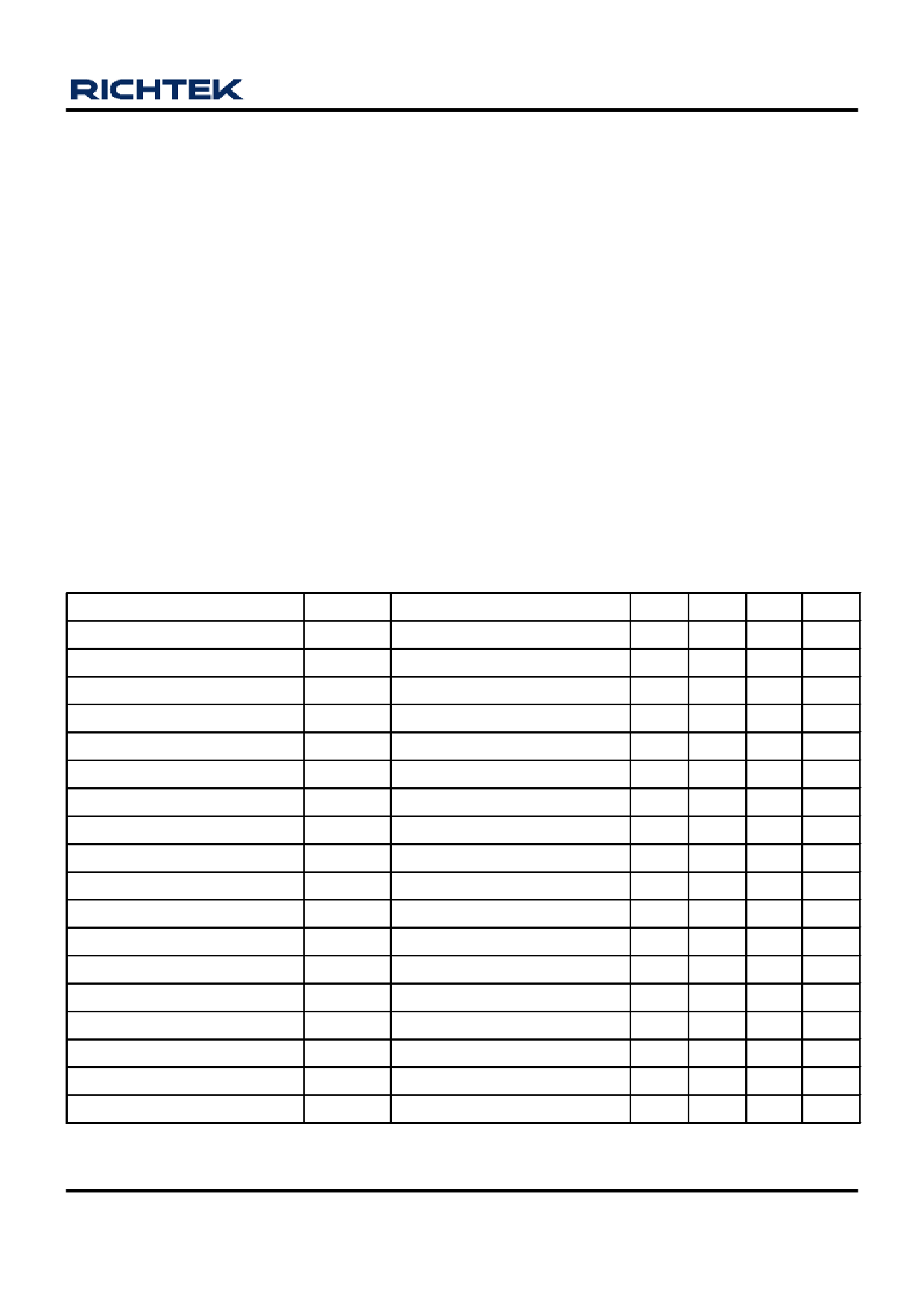
Electrical Characteristics
(VIN = 1.5V, VDD set to 3.3V, Load Current = 0, TA = 25° C, unless otherwise specified)
Parameter
Symbol
Test Conditions
Start-UP Voltage
Operating VDD Range
Shutdown Current I (VIN)
Switch-off Current I (VDD)
Continuous Switching Current
VST
IL = 1mA
VDD
VDD pin voltage
IOFF
EN Pin = 0V, VIN = 4.5V
ISWITCH OFF VIN = 6V
ISWITCH
VIN = EN = 3.3V, VFB = GND
No Load Current I (VIN)
Feedback Reference Voltage
Switching Frequency
Maximum Duty
LX ON Resistance
Current Limit Setting
EXT ON Resistance to VDD
EXT ON Resistance to GND
Line Regulation
Load Regulation
EN Pin Trip Level
Temperature Stability for Vout
Thermal Shutdown Hysterises
INO LOAD
VREF
FS
DMAX
ILIMIT
∆VLINE
∆VLOAD
TS
∆TSD
VIN = 1.5V, VOUT = 3.3V
Close Loop, VDD = 3.3V
VDD = 3.3V
VDD = 3.3V
VDD = 3.3V
VDD = 3.3V
VDD = 3.3V
VDD = 3.3V
VIN = 3.5 ~ 6V, IL = 1mA
VIN = 2.5V, IL = 1 ~ 100mA
VDD = 3.3V
Min Typ Max Units
-- 0.98 1.05 V
2
--
6
V
-- 0.01 1
µA
--
17
25
µA
0.4 0.55 0.7 mA
--
75*
--
µA
1.225 1.25 1.275 V
425 500 575 kHz
85 95
--
%
--
0.3 1.1
Ω
1.6
2
2.6**
A
--
5
8.5
Ω
--
5
8.5
Ω
--
1.5 10 mV/V
-- 0.25*** -- mV/mA
0.4 0.8 1.2
V
--
50
-- ppm/°C
--
10
--
°C
DS9266-12 May 2007
www.richtek.com
5
Share Link: 