RFD8P05 데이터 시트보기 (PDF) - Intersil
부품명
상세내역
일치하는 목록
RFD8P05 Datasheet PDF : 6 Pages
| |||
RFD8P05, RFD8P05SM, RFP8P05
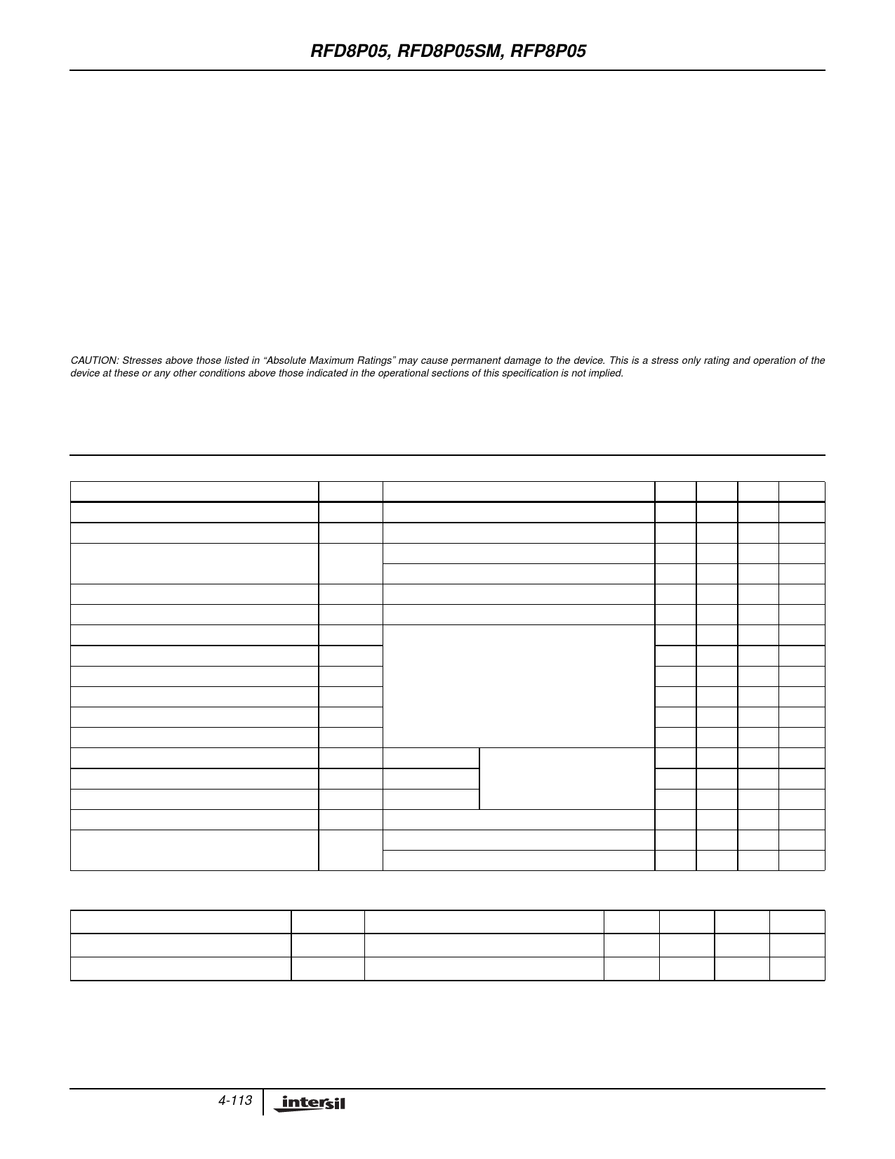
Absolute Maximum Ratings TC = 25oC Unless Otherwise Specified
Drain to Source Voltage (Note 1) . . . . . . . . . . . . . . . . . . . . . . . . . . . . . . . . . . . . . . . . . . . . . VDSS
Drain to Gate Voltage (RGS = 20KΩ) (Note 1). . . . . . . . . . . . . . . . . . . . . . . . . . . . . . . . . . .VDGR
Continuous Drain Current . . . . . . . . . . . . . . . . . . . . . . . . . . . . . . . . . . . . . . . . . . . . . . . . . . . . .ID
Pulsed Drain Current (Note 3) . . . . . . . . . . . . . . . . . . . . . . . . . . . . . . . . . . . . . . . . . . . . . . . . IDM
Gate to Source Voltage . . . . . . . . . . . . . . . . . . . . . . . . . . . . . . . . . . . . . . . . . . . . . . . . . . . . . VGS
Maximum Power Dissipation . . . . . . . . . . . . . . . . . . . . . . . . . . . . . . . . . . . . . . . . . . . . . . . . . . PD
Dissipation Derating Factor . . . . . . . . . . . . . . . . . . . . . . . . . . . . . . . . . . . . . . . . . . . . . . . . . . . . .
RFD8P05,
RFD8P05SM, RFP8P05
-50
-50
-8
-20
±20
48
0.27
UNITS
V
V
A
A
V
W
W/oC
Single Pulse Avalanche Energy Rating . . . . . . . . . . . . . . . . . . . . . . . . . . . . . . . . . . . . . . . . . EAS
See Figure 6
Operating and Storage Temperature . . . . . . . . . . . . . . . . . . . . . . . . . . . . . . . . . . . . . . . TJ, TSTG
-55 to 175
oC
Maximum Temperature for Soldering
Leads at 0.063in (1.6mm) from Case for 10s. . . . . . . . . . . . . . . . . . . . . . . . . . . . . . . . . . . . TL
Package Body for 10s, See Techbrief 334 . . . . . . . . . . . . . . . . . . . . . . . . . . . . . . . . . . . . .Tpkg
300
260
oC
oC
CAUTION: Stresses above those listed in “Absolute Maximum Ratings” may cause permanent damage to the device. This is a stress only rating and operation of the
device at these or any other conditions above those indicated in the operational sections of this specification is not implied.
NOTE:
1. TJ = 25oC to 150oC.
Electrical Specifications TC = 25oC Unless Otherwise Specified
PARAMETER
SYMBOL
TEST CONDITIONS
Drain to Source Breakdown Voltage
Gate Threshold Voltage
Zero Gate Voltage Drain Current
Gate to Source Leakage Current
Drain to Source On Resistance (Note 2)
Turn-On Time
Turn-On Delay Time
Rise Time
Turn-Off Delay Time
Fall Time
Turn-Off Time
Total Gate Charge
Gate Charge at -5V
Threshold Gate Charge
Thermal Resistance Junction to Case
Thermal Resistance Junction to Ambient
BVDSS
VGS(TH)
IDSS
IGSS
rDS(ON)
tON
td(ON)
tr
td(OFF)
tf
tOFF
Qg(TOT)
Qg(-10)
Qg(TH)
RθJC
RθJA
ID = 250µA, VGS = 0V (Figure 9)
VGS = VDS, ID = 250µA (Figure 8)
VDS = Rated BVDSS, VGS = 0V
VDS = 0.8 x Rated BVDSS, TJ = 150oC
VGS = ±20V
ID = 8A, VGS = -10V (Figure 7)
VDD = -25V, ID ≈ 4A, RG = 9.1Ω, RL = 6.25Ω,
VGS = -10V
VGS = 0 to -20V
VGS = 0 to -10V
VGS = 0 to -2V
VDD = -40V, ID = 8A,RL = 5Ω,
IG(REF) = -0.3mA
TO-251AA, TO-252AA
TO-220AB
MIN TYP MAX UNITS
-50
-
-
V
-2
-
-4
V
-
-
1
µA
-
-
25
µA
-
- ±100 nA
-
- 0.300 Ω
-
-
60
ns
-
16
-
ns
-
30
-
ns
-
42
-
ns
-
20
-
ns
-
- 100 ns
-
-
80 nC
-
-
40 nC
-
-
2
nC
-
- 3.125 oC/W
-
-
100 oC/W
62.5 oC/W
Source to Drain Diode Specifications TC = 25oC Unless Otherwise Specified
PARAMETER
SYMBOL
TEST CONDITIONS
Source to Drain Diode Voltage (Note 2)
VSD
ISD = -8A
Reverse Recovery Time
trr
ISD = -8A, dISD/dt = 100A/µs
NOTE:
2. Pulse test: pulse width ≤ 300µs, Duty Cycle ≤ 2%.
3. Repetitive rating: pulse width is limited by maximum junction temperature.
MIN
TYP
MAX UNITS
-
-
-1.5
V
-
-
125
ns
4-113
Share Link: 