R3115Z 데이터 시트보기 (PDF) - RICOH Co.,Ltd.
부품명
상세내역
일치하는 목록
R3115Z Datasheet PDF : 28 Pages
| |||
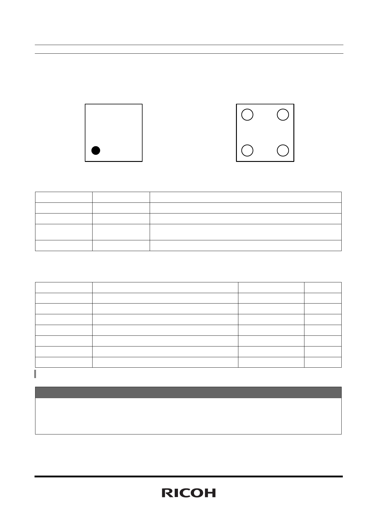
PIN CONFIGURATIONS
Mark Side
4
3
WLCSP-4-P2
R3115Z
Bump Side
3
4
1
2
2
1
PIN DESCRIPTIONS
Pin No.
1
2
Symbol
GND
CD
3
OUT
4
VDD
Description
Ground Pin
Pin for External Capacitor (for setting output delay)
Output Pin
(Output “L” at detector threshold, Output “H” atreleased voltage)
Supply Voltage Pin
ABSOLUTE MAXIMUM RATINGS
Symbol
VDD
VOUT1
VOUT2
IOUT
PD
Topt
Tstg
Item
Supply Voltage
Output Voltage (CMOS)
Output Voltage (Nch)
Output Current
Power Dissipation(WLCSP-4-P2)*1
Operating Temperature Range
Storage Temperature Range
Rating
6.5
VSS−0.3 to VDD+0.3
VSS−0.3 to 6.5
20
530
−40 to 85
−55 to 125
Unit
V
V
V
mA
mW
°C
°C
1) For Power Dissipation, please refer to PACKAGE INFORNATION to be described.
ABSOLUTE MAXIMUM RATINGS
Absolute Maximum ratings are threshold limit values that must not be exceeded ever for an instant under
any conditions. Moreover, such values for any two items must not be reached simultaneously. Operation
above these absolute maximum ratings may cause degradation or permanent damage to the device.
These are stress ratings only and do not necessarily imply functional operation below these limits.
3
Share Link: 