PJ7915CI 데이터 시트보기 (PDF) - Promax Johnton
부품명
상세내역
일치하는 목록
PJ7915CI Datasheet PDF : 9 Pages
| |||
PJ7900 Series
3-Terminal Negative Output Voltage Regulators
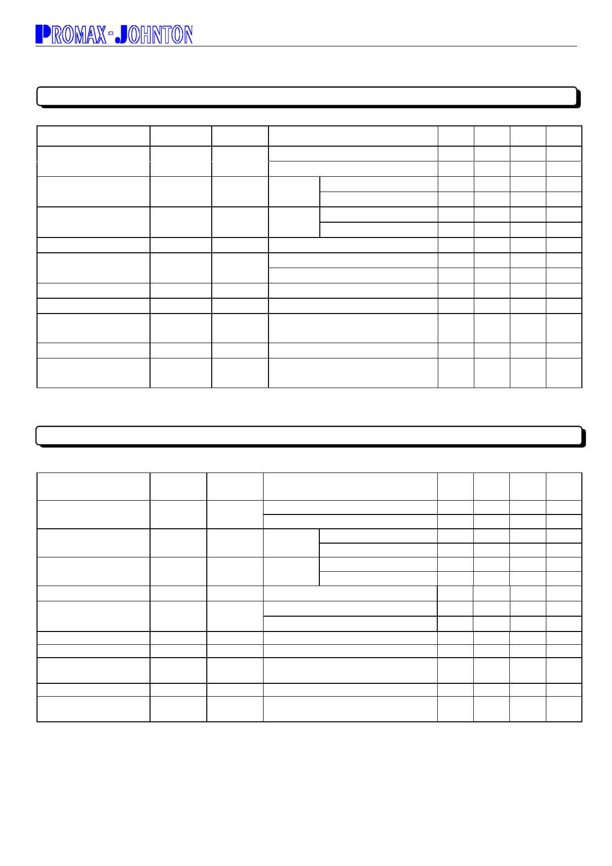
• PJ7906 ELECTRICAL CHARACTERISTICS
(Vin=-11V, Iout=500mA, Cin=2μF, Cout=1μF; Tj=0℃ to 125℃, unless otherwise specified.)
CHARACTERISTIC
Output Voltage
Line Regulation
Load Regulation
Quiescent Current
Quiescent Current Change
Output Noise Voltage
SYMBOL
Vo
REGline
REGload
Iq
ΔIq
Vn
TEST
CIRCUIT
1
1
1
2
2
1
CONDITION
Tj=25℃
Vi=-8 to -21V, lo=5mA to 1A, PD<15W
Tj=25℃ Vi=-8 to -25V
Tj=25℃
Vi=-9 to -13V
Io=5mA to 1.5A
Io=250mA to 750mA
Tj=25℃
Vi=-8 to -25V, Tj=25℃
lo=5mA to 1A, Tj=25℃
f=10Hz to 100KHz, Ta=25℃
MIN.
-5.75
-5.70
--
--
--
--
--
--
--
--
TYP.
-6.0
-6.0
4
1.5
10
3
2
--
--
44
MAX.
-6.25
-6.30
120
60
120
60
4
1.3
0.5
--
UNIT
V
V
mV
mV
mV
mV
mA
mA
mA
μV
Ripple Rejection Ratio
RR
3
Vi=-9 to -19V, Io=100mA, f=120Hz
60
73
--
dB
Min. I/O Voltage
Difference
Peak Output Current
Vdif
Io-peak
Io=1A, Tj=25℃
1
Tj=25℃
--
1.1
--
V
--
2.1
--
A
Output Voltage
Tempoerature Coefficient
ΔVo/Ta
1
Io=5mA, Tj=0 to 125℃
mV/
--
-0.5
--
℃
Note: The specified condition Tj=25℃ means that the test should be carried out with the test time so short (within 10mS), that the drift in
characteristic value due to the rise in chip junction temperature can be ignored.
• PJ7908 ELECTRICAL CHARACTERISTICS
(Vin=-14V, Iout=500mA, Cin=2μF, Cout=1μF; Tj=0℃ to 125℃, unless otherwise specified.)
CHARACTERISTIC
Output Voltage
Line Regulation
Load Regulation
SYMBOL
Vo
REGline
REGload
TEST
CIRCUIT
1
1
1
CONDITION
Tj=25℃
Vi=-10.5 to -23V, lo=5mA to 1A, PD<15W
Tj=25℃ Vi=-10.5 to -25V
Tj=25℃
Vi=-11 to -17V
Io=5mA to 1.5A
Io=250mA to 750mA
MIN.
-7.69
-7.61
--
--
--
--
TYP.
-8.0
-8.0
6
2
12
4
MAX. UNIT
-8.32 V
-8.40 V
160 mV
80
mV
160 mV
80
mV
Quiescent Current
Iq
2
Tj=25℃
--
2
4
mA
Quiescent Current Change
ΔIq
Output Noise Voltage
Vn
2
Vi=-10.5 to -25V, Tj=25℃
lo=5mA to 1A
1
f=10Hz to 100KHz, Ta=25℃
--
--
1
mA
--
--
0.5 mA
--
52
--
μV
Ripple Rejection Ratio
RR
3
Vi=-11 to -21V, Io=100mA, f=120Hz
56
71
--
dB
Min. I/O Voltage
Difference
Peak Output Current
Vdif
Io-peak
Io=1A, Tj=25℃
1
Tj=25℃
--
2
--
V
--
2.1
--
A
Output Voltage
Tempoerature Coefficient
ΔVo/Ta
1
Io=5mA, Tj=0 to 125℃
mV/
--
-0.6
--
℃
Note: The specified condition Tj=25℃ means that the test should be carried out with the test time so short (within 10mS), that the drift in
characteristic value due to the rise in chip junction temperature can be ignored.
3-9
2002/10.rev.A
Share Link: 