74ACT299SC 데이터 시트보기 (PDF) - Fairchild Semiconductor
부품명
상세내역
일치하는 목록
74ACT299SC
Fairchild Semiconductor

74ACT299SC Datasheet PDF : 11 Pages
| |||
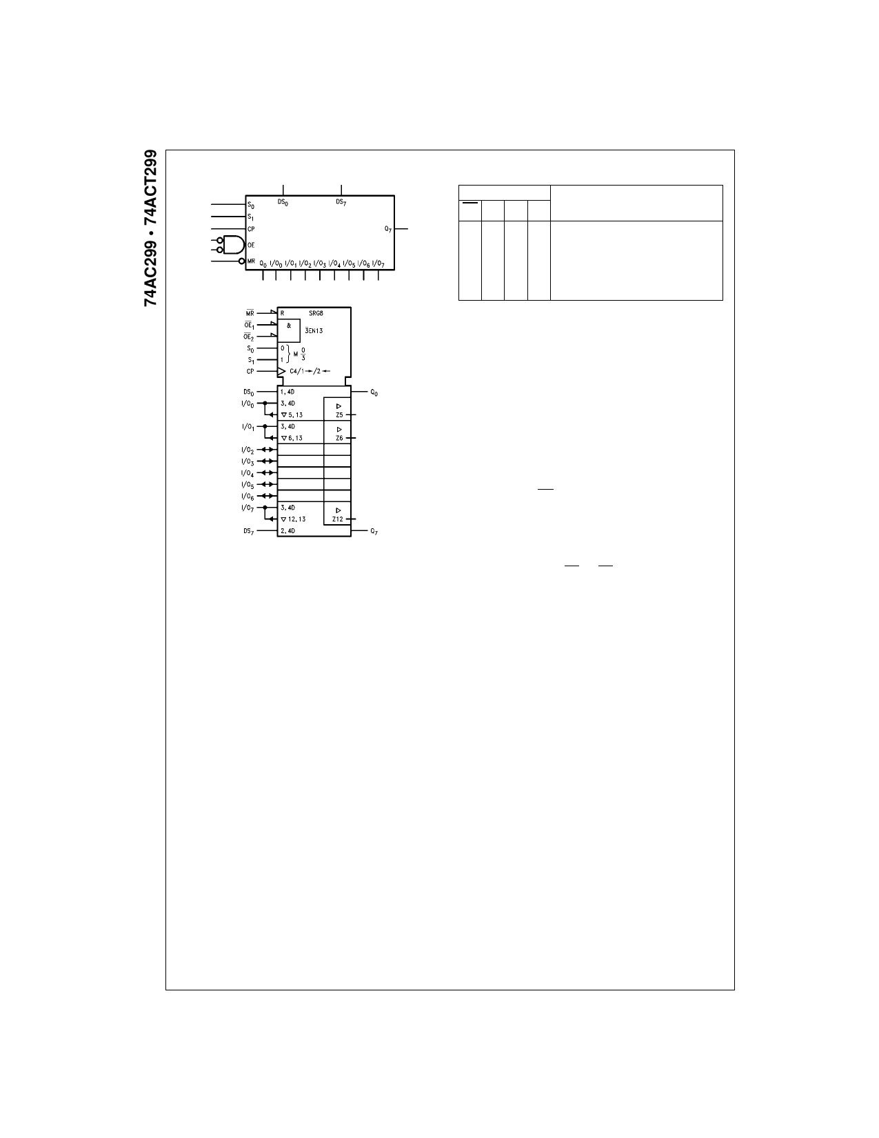
Logic Symbols
IEEE/IEC
Truth Table
Inputs
Response
MR S1 S0 CP
L
H
H
H
X
H
L
H
X
H
H
L
X Asynchronous Reset; Q0–Q7 LOW
Parallel Load; I/On o Qn
Shift Right; DS0 o Q0, Q0 o Q1, etc.
Shift Left, DS7 o Q7, Q7 o Q6, etc.
H L L X Hold
H HIGH Voltage Level
L LOW Voltage Level
X Immaterial
LOW-to-HIGH Transition
Functional Description
The AC/ACT299 contains eight edge-triggered D-type flip-
flops and the interstage logic necessary to perform syn-
chronous shift left, shift right, parallel load and hold opera-
tions. The type of operation is determined by S0 and S1, as
shown in the Truth Table. All flip-flop outputs are brought
out through 3-STATE buffers to separate I/O pins that also
serve as data inputs in the parallel load mode. Q0 and Q7
are also brought out on other pins for expansion in serial
shifting of longer words.
A LOW signal on MR overrides the Select and CP inputs
and resets the flip-flops. All other state changes are initi-
ated by the rising edge of the clock. Inputs can change
when the clock is in either state provided only that the rec-
ommended setup and hold times, relative to the rising edge
of CP, are observed.
A HIGH signal on either OE1 or OE2 disables the 3-STATE
buffers and puts the I/O pins in the high impedance state.
In this condition the shift, hold, load and reset operations
can still occur. The 3-STATE buffers are also disabled by
HIGH signals on both S0 and S1 in preparation for a paral-
lel load operation.
www.fairchildsemi.com
2
Share Link: