74ACT299 데이터 시트보기 (PDF) - Fairchild Semiconductor
부품명
상세내역
일치하는 목록
74ACT299
Fairchild Semiconductor

74ACT299 Datasheet PDF : 11 Pages
| |||
July 1988
Revised March 2005
74AC299 • 74ACT299
8-Input Universal Shift/Storage Register
with Common Parallel I/O Pins
General Description
The AC/ACT299 is an 8-bit universal shift/storage register
with 3-STATE outputs. Four modes of operation are possi-
ble: hold (store), shift left, shift right and load data. The par-
allel load inputs and flip-flop outputs are multiplexed to
reduce the total number of package pins. Additional out-
puts are provided for flip-flops Q0, Q7 to allow easy serial
cascading. A separate active LOW Master Reset is used to
reset the register.
Features
s ICC and IOZ reduced by 50%
s Common parallel I/O for reduced pin count
s Additional serial inputs and outputs for expansion
s Four operating modes: shift left, shift right, load
and store
s 3-STATE outputs for bus-oriented applications
s Outputs source/sink 24 mA
s ACT299 has TTL-compatible inputs
Ordering Code:
Order Number Package Number
Package Description
74AC299SC
M20B
20-Lead Small Outline Integrated Circuit (SOIC), JEDEC MS-013, 0.300" Wide
74AC299SCX_NL
(Note 1)
M20B
Pb-Free 20-Lead Small Outline Integrated Circuit (SOIC), JEDEC MS-013, 0.300"
Wide
74AC299SJ
M20D
Pb-Free 20-Lead Small Outline Package (SOP), EIAJ TYPE II, 5.3mm Wide
74AC299MTC
MTC20
20-Lead Thin Shrink Small Outline Package (TSSOP), JEDEC MO-153, 4.4mm Wide
74AC299PC
N20A
20-Lead Plastic Dual-In-Line Package (PDIP), JEDEC MS-001, 0.300" Wide
74ACT299SC
M20B
20-Lead Small Outline Integrated Circuit (SOIC), JEDEC MS-013, 0.300" Wide
74ACT299MTC
MTC20
20-Lead Thin Shrink Small Outline Package (TSSOP), JEDEC MO-153, 4.4mm Wide
74ACT299PC
N20A
20-Lead Plastic Dual-In-Line Package (PDIP), JEDEC MS-001, 0.300" Wide
Device also available in Tape and Reel. Specify by appending suffix letter “X” to the ordering code.
Pb-Free package per JEDEC J-STD-020B.
Note 1: “_NL” indicates Pb-Free package (per JEDEC J-STD-020B). Device available in Tape and Reel only.
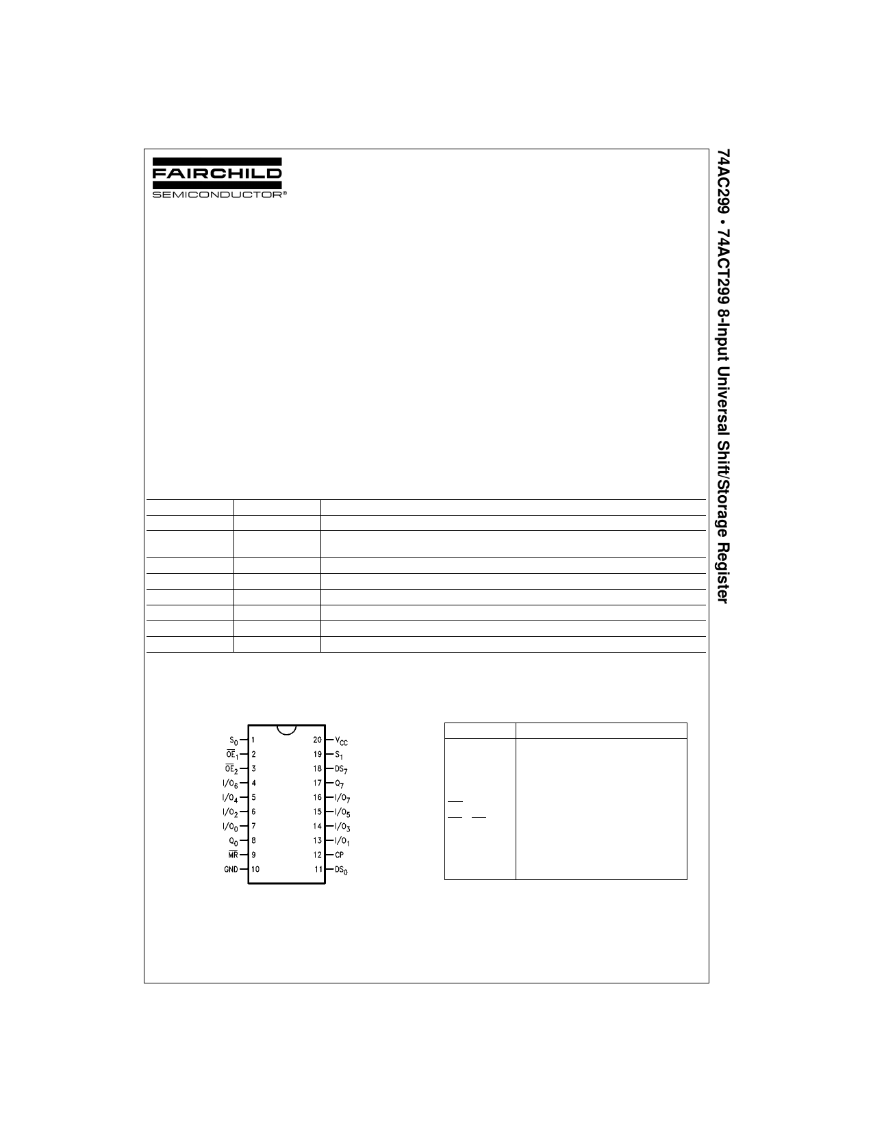
Connection Diagram
Pin Descriptions
Pin Names
CP
DS0
DS7
S0, S1
MR
OE1, OE2
I/O0–I/O7
Q0, Q7
Description
Clock Pulse Input
Serial Data Input for Right Shift
Serial Data Input for Left Shift
Mode Select Inputs
Asynchronous Master Reset
3-STATE Output Enable Inputs
Parallel Data Inputs or
3-STATE Parallel Outputs
Serial Outputs
FACT¥ is a trademark of Fairchild Semiconductor Corporation.
© 2005 Fairchild Semiconductor Corporation DS009893
www.fairchildsemi.com
Share Link: