LC86E5032 데이터 시트보기 (PDF) - SANYO -> Panasonic
부품명
상세내역
일치하는 목록
LC86E5032 Datasheet PDF : 21 Pages
| |||
LC86E5032
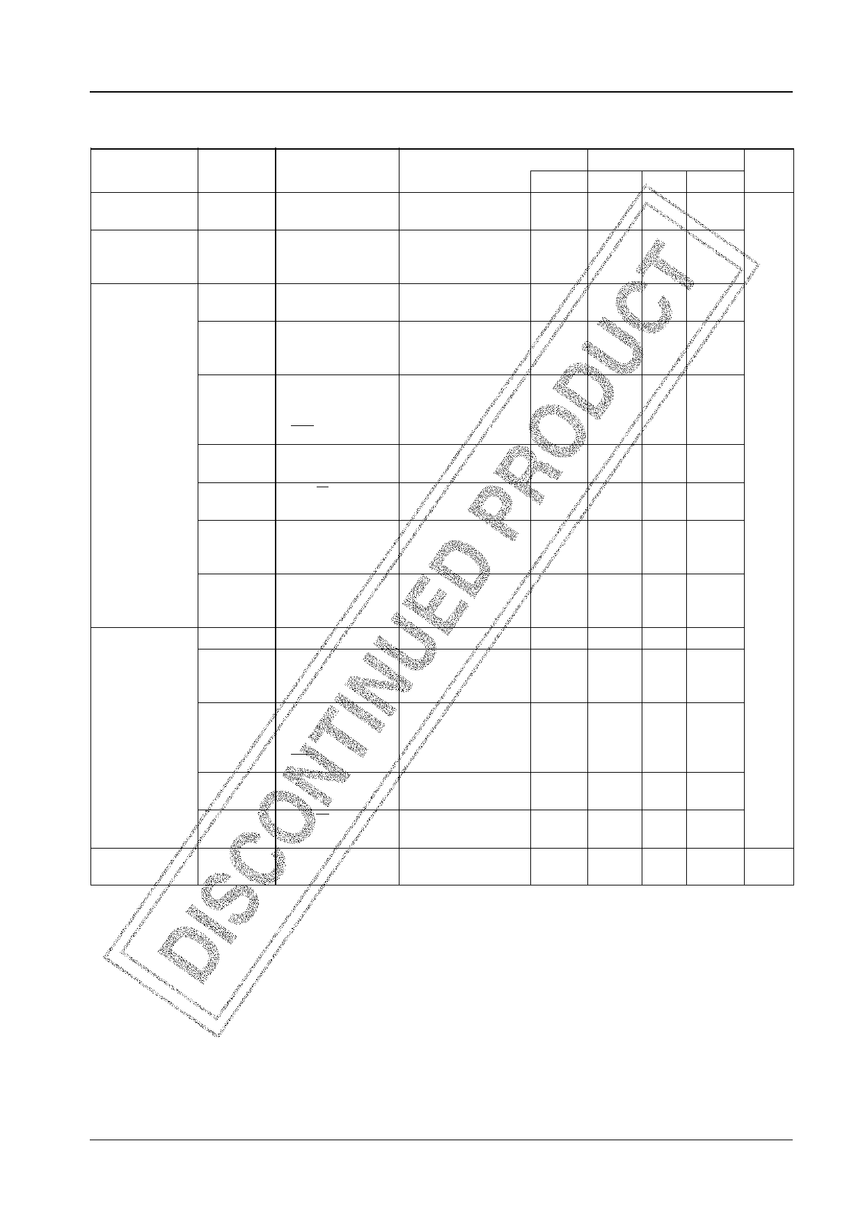
2. Recommended Operating Range at Ta = +10°C to +40°C, VSS = 0 V
Parameter
Operating voltage
range
HOLD voltage
Input high
voltage
Input low
voltage
Operation cycle
time
Symbol
VDD(1)
VHD
VIH(1)
VIH(2)
VIH(3)
VIH(4)
VIH(5)
VIH(6)
VIH(7)
VIL(1)
VIL(2)
VIL(3)
VIL(4)
VIL(5)
tCYC
Pins
Conditions
Ratings
Unit
VDD[V] min
typ
max
VDD
0.98 µs ≤ tCYC
tCYC ≤ 400 µs
4.5
6.0 V
VDD
RAM and registers
2.0
6.0
retain their pre-HOLD
mode values.
Port 0 (Schmitt)
Output disabled
4.5 to 6.0 0.4VDD
VDD
+0.9
• Ports 1, 2
Output disabled
4.5 to 6.0 0.75VDD
VDD
• Ports 72, 73
(Schmitt)
• Port 70
Output N-channel
4.5 to 6.0 0.75VDD
VDD
Port input/interrupt. transistor OFF
• Port 71
• RES (Schmitt)
Port 70
Output N-channel
4.5 to 6.0 0.9VDD
VDD
Watchdog timer
transistor OFF
• Port 74
Output N-channel
4.5 to 6.0 0.75VDD
VDD
• Port 8
transistor OFF
Ports 3, 4, 5 of
Output disabled
4.5 to 6.0 0.75VDD
VDD
CMOS output
(Schmitt)
Ports 3, 4, 5 of open
drain output
(Schmitt)
Output disabled
4.5 to 6.0 0.75VDD
13.5
Port 0 (Schmitt) Output disabled
4.5 to 6.0
VSS
0.2VDD
• Ports 1, 2, 3, 4, 5
• Ports 72, 73
(Schmitt)
Output disabled
4.5 to 6.0
VSS
0.25VDD
• Port 70
N-channel transistor 4.5 to 6.0
VSS
Port input/interrupt. OFF
• Port 71
• RES (Schmitt)
0.25VDD
Port 70
Watchdog timer
N-channel transistor 4.5 to 6.0
VSS
OFF
0.8VDD
–1.0
• Port 74
• Port 8
N-channel transistor 4.5 to 6.0
VSS
OFF
0.25VDD
4.5 to 6.0 0.98
400 µs
No. 5632-11/21
Share Link: 