PI6C2404A 데이터 시트보기 (PDF) - Pericom Semiconductor
부품명
상세내역
일치하는 목록
PI6C2404A Datasheet PDF : 6 Pages
| |||
PI6C2404A-1 1122334455667788990011223344556677889900112233445566778899001122112233445566778899001122334455667788990011223344556677889900112211223344556677889900112233445566778899001122334455667788990011221122334455667788990011223344556677889900112233445566778899001122112233445566778899001122
Zero-Delay Clock Buffer
Features
• Maximum rated frequency: 133 MHz
• Low cycle-to-cycle jitter
• Input to output delay, less than 200ps
• External feedback pin allows outputs to be synchronized
to the clock input
• 5V tolerant input*
• Operates at 3.3V VDD
• Test mode allows bypass of the PLL for system testing
purposes (e.g., IBIS measurements)
• Space-saving Packaging (Pb-free and Green Available):
— 8-pin, 150-mil SOIC (W)
Description
The PI6C2404A-1 is a PLL-based, zero-delay buffer, with the ability
to distribute four outputs of up to 133 MHz at 3.3V. Two banks of
two outputs exist, OUTA[1–2] and OUTB[1–2].
An external feedback pin is used to synchronize the outputs to the
input; the relationship between loading of this signal and the other
outputs determines the input-output delay.
The PI6C2404A-1 is characterized for both commercial and industrial
operation.
* FB_IN and CLKIN must reference the same voltage thresh-
olds for the PLL to deliver zero delay skewing
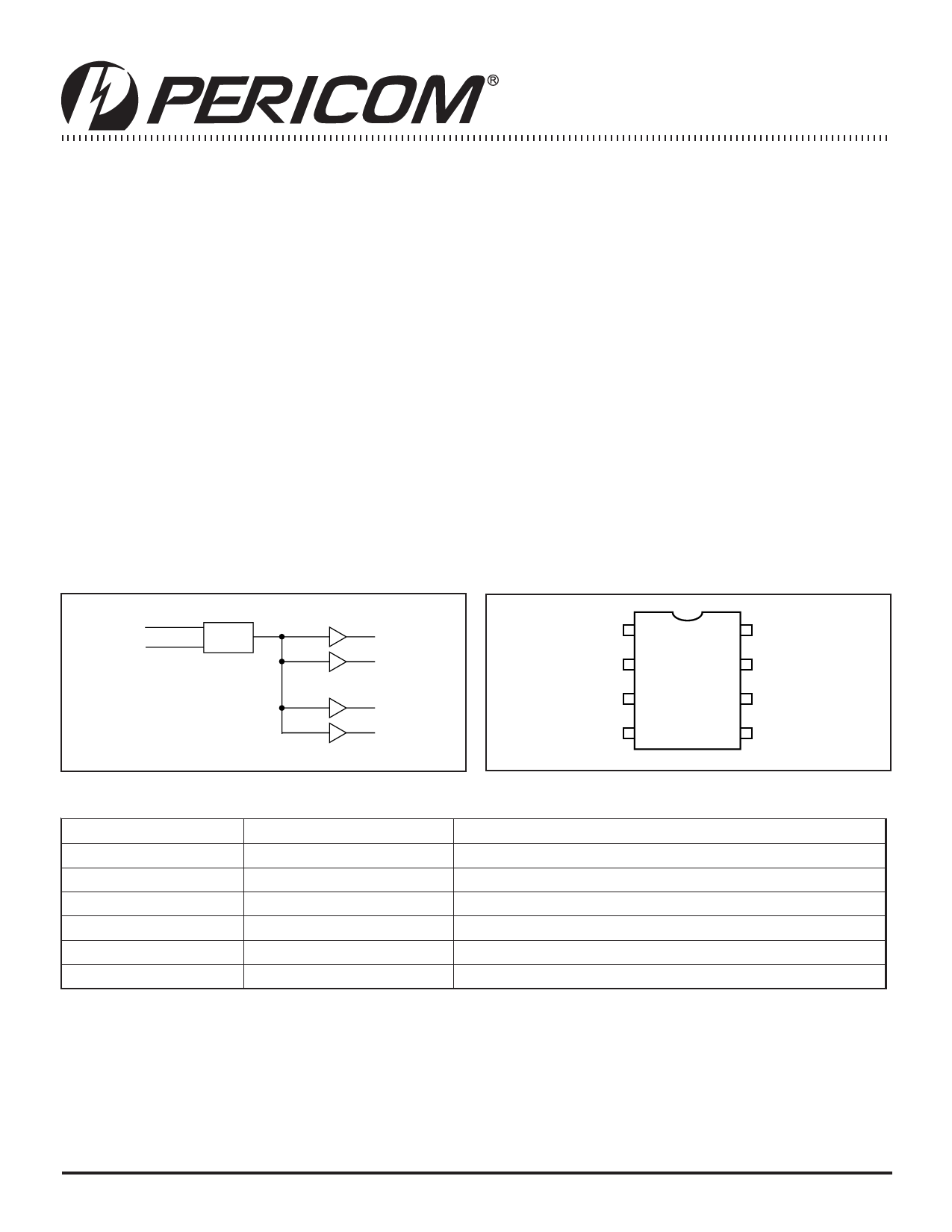
Block Diagram
FB_IN
CLKIN
PLL
OUTA1
OUTA2
OUTB1
OUTB2
Pin Configuration
CLKIN 1
8 FB_IN
OUTA1 2 8-Pin 7 VDD
W
OUTA2 3
6 OUTB2
GND 4
5 OUTB1
Pin Description
Pin
1
2, 3
7
4
5, 6
8
Signal
CLKIN
OUTA[1-2]
VDD
GND
OUTB[1-2]
FB_IN
Description
Input clock reference frequency (weak pull-down)
Clock output, Bank A
3.3V supply
Ground
Clock output, Bank B
PLL feedback input
06-0036
1
PS8609A 01/13/05
Share Link: 